Download
1 / 14
140 likes | 173 Views
Explore the latest developments and applications of 3D technology, focusing on radiation-hard detectors for experiments like IBL, TOTEM, LHCb, and more. Discover the fabrication processes, new designs, and collaborative efforts in the field.

E N D
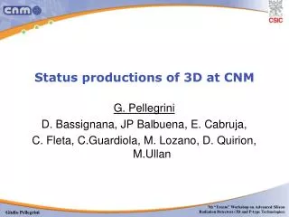
Status of 3D detector productions at CNM Giulio Pellegrini Instituto de Microelectrónica de Barcelona, IMB-CNM-CSIC, Barcelona, Spain
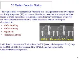
Hole aspect ratio 25:1 10µm diameter, 250µm deep P- and N-type substrates, 285µm thick Double-sided 3D at CNM • Columns etched from opposite sides of substrate and don't pass through full thickness • All fabrication done in-house • ICP is a reliable and repeatable process (many successful runs) Electrode fabrication: ICP etching of the holes: Bosch process, ALCATEL 601-E Holes partially filled with LPCVD poly Doping with P or B Holes passivated with TEOS SiO2 Devices designed and fabricated at CNM
Applications and experiments interested in 3D technology • IBL and Atlas upgrade • TOTEM • LHCb experiment • Stripixels • Flip chip
Radiation-hard 3D detectors for the (s)LHC • Inner pixel layer (IBL) replacement for ATLAS • Fluence of 4.4 x 10¹⁵ 1MeV neq/cm2 • Super-LHC – Atlas and CMS • 10 * luminosity upgrade on present LHC • Fluence up to ~ 1 x 10¹⁶ 1MeV neq/cm2 • LHCb VELO upgrade • Integrated fluence ~ 1 x 10¹⁶ 1MeV neq/cm2 • TOTEM experiment • Integrated fluence ~ 1 x 10¹⁶ 1MeV neq/cm2 • Design fluences for ATLAS sensors (includes 2x safety factor) : • Innermost Pixel Layer ~ 5cm radius :1.6 x 10¹⁶ 1MeV neq/cm2 = 500 Mrad • Outer Pixel Layers ~ 30cm radius: 3 x 10¹⁵ 1MeV neq/cm2 = 150 Mrad
Atlas pixels FE-I4 Atlas pixels, FE-I3 and new FE-I4 fabrication and irradiation for Insertable B-Layer and testbeam. In the framework of the Atlas 3D collaboration (http://test-3dsensor.web.cern.ch/test-3dsensor/). Common layout in the Atlas 3D collaboration (CNM, FBK, SINTEF, Stanford). New FE-I4 design (2x2 cm2). A module should be fabricated with 3D detectors. First run with 18 wafers, double side configuration. • 10 225um 4” thick wafers • 8 300um 4” thick wafers • Status: Doping first set of holes. Second run with 18 wafers, single side configuration • 18 SOI 4” wafers, 225um thick • Status: starting this week Work done with IFAE and Glasgow Uni.
Old mask with different devices New run in production We have only 2 wafers left due to perforation problems Wafers will be ready by next week. To be tested and bonded, priority for FE-I3 devices Atlas pixels FE-I3 Wafer perforation during DRIE is due to unintentional openings (defects) in aluminum mask whose surface is larger than hole surface.
CMS 3D pixels We have designed a new mask with single chips and one module 8x2. We are also implementing a new bias grid for 3D detectors without punch trough. Fabrication started at CNM. Status etching first set of holes. Work done with PSI and IFCA.
TOTEM 3D strips We have designed a new mask to fabricate TOTEM strip detectors with 3D technology. Status: approval of the mask • Strip pitch 66um • AC coupled. • 3cm long • p+ readout Work done with CERN.
LHCb upgrade with 3D pixel detectors • Use of Medipix3 for the future LHCb upgrade. Full pixel detector matrix. • Secondary 120 GeV pion beam from SPS • 4 Timepix, 2 Medipix planes in telescope • DUT: double sided 3D N-type sensor from CNM/Glasgow • Expected track extrapolation error: < 3 μm 6 medipix2 3d irradiated with neutrons and bump bonded with Timepix. Status: new fabrication run will finish next week Pion beam Individual pion tracks Measurements at 0º, done. Results with scan to 10º : see Chris´s talk Work done with Glasgow. telescope DUT Double sided 3D sensors compatible with standard pixel read out electronics. High voltage on the back of the pixels like in planar devices.
Stripixels 3D strip detectors with 2D positioning on one side. Double metal process. Mask already designed, detectors are being fabricated at CNM. Status: patterning second poly. Work done with Brookhaven National Laboratory .
Flip-Chip • Flip-chip technology is now available commercially at CNM facilities through the spin-off X-ray Imatek. • Extended work done with Medipix2 and Atlas FE-I3 and FE-I4 (dummies) read out pixel chips. • Techniques: • High density Flip-chip • Sn/Ag, Sn/Pb bumping • Equipment: • ATV reflow oven with vacuum • SET FC150 flip chip machine • UBM deposited with an electroless method CERN Courier 2010
Dummies FE-I4 CNM already fabricated 24 6” wafers to test the bump bonding with Sn/Ag at CNM and 8 4” wafers to test the bump bonding with In at SELEX. Dummies include one structure to test pixels detectors with ALIBAVA read out electronics. Wafers were also thinned at IZM and are now tested at CNM and Genova. First results very positives, >99,98% yield. Although FE-I4 dummy has only one metal! 6” wafer
Sensor thinning • Collaboration with Universidad de Santiago for the LHCb experiment to thin 2D-pixel (55x55 μm) sensor from 300 μm down to 200, 150, 100 μm, p-on-n & n-on-p (with p-spray) • Read out with TimePix and MPX3 ASICs (SnAg) • Goal: • Measure resolution, efficiency, … thin sensor • Minimal guard ring design. • Production of module/ladder with 3 ASICs 55Fe Abraham Gallas Timepix on SOI 150mm 13 26/10/10 Abraham Gallas
Conclusions • 3D Technology available at CNM for different configurations • Different CERN experiments are interested in 3D technology • We have dummy samples for flip chip testing of FE-I4 devices • Flip-chip is now available commercially.