Download
1 / 54
540 likes | 755 Views
AD vanced. MO nolithic. S ensors for. Radiation damage effects in Monolithic Active Pixel Sensors Implemented in an 0.18µm CMOS process Dennis Doering, Goethe-University Frankfurt am Main on behalf of the CBM-MVD- Collaboration. O utline MAPS sensors

E N D
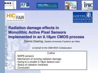
ADvanced MOnolithic Sensors for Radiation damageeffects in MonolithicActive Pixel Sensors Implemented in an 0.18µm CMOS process Dennis Doering, Goethe-University Frankfurt am Main on behalf ofthe CBM-MVD-Collaboration • Outline • MAPS sensors • Mechanismofionizingradiationdamage • Goingto a smaller 0.18µm featuresize • Status ofradiationhardness • Conclusion
Applicationsof MAPS MAPS are developed for applications as vertex detector since 1999 at IPHC (Strasbourg). Picture STAR STAR-Experiment Possible ITS-Upgrade ALICE Picture CBM International Linear Collider CBM-Experiment (FAIR, GSI) Dennis Doering: MAPS in 0.18µm CMOS process DPG Dresden March 2013
Operation principle of MAPS +3.3V Output Source Follower SiO2 P-Well P+ Diode N+ Epitaxial Layer P- P+ Dennis Doering: MAPS in 0.18µm CMOS process DPG Dresden March 2013
Noise measurement Measurednoise [mV] +3.3V Output Readoutchain Gain ENC [e] • Measurednoise [mV] attheoutput • Charge-to-voltageconversionbythereadoutchaingain • Calculate ENC [e] Dennis Doering: MAPS in 0.18µm CMOS process DPG Dresden March 2013
Classesof radiation damage To be investigated and improved: Radiation hardness against… • … non-ionizing radiation: • Energy deposited into the crystal lattice • Atoms are displaced • Caused by heavy (fast leptons, hadrons),charged and neutral particles DPG Mainz 2012 HK 12.8 ~1014neq with high-resistivity sensor Farnan I, HM Cho, WJ Weber, 2007. "Quantification of Actinide α-Radiation Damage in Minerals and Ceramics." Nature 445(7124):190-193. Discussed in this talk • … ionizing radiation: • Energy deposited into the electron cloud • Can ionize atoms and destroy molecules • Caused by charged particles and photons Dennis Doering: MAPS in 0.18µm CMOS process DPG Dresden March 2013
Ionizingradiationdamageeffects Measurednoise [mV] +3.3V Output Gain ENC [e] Ionizingradiationdamagegenerateselectronsat Si/SiO2 interface Leakagecurrentand ENC [e] increases Gainisconstant Measurednoise [mV] increases Dennis Doering: MAPS in 0.18µm CMOS process DPG Dresden March 2013
Goingtosmallerfeaturesize „new“ 0.18µm CMOS process 0.35µm CMOS process Mindthe different scale! Measurednoise [mV] decreases! Dennis Doering: MAPS in 0.18µm CMOS process DPG Dresden March 2013
Goingtosmallerfeaturesize „new“ 0.18µm CMOS process 0.35µm CMOS process Mindthe different scale! Measurednoise [mV] decreases! Reason: Gaindrops after 10Mrad Dennis Doering: MAPS in 0.18µm CMOS process DPG Dresden March 2013
Goingtosmallerfeaturesize „new“ 0.18µm CMOS process 0.35µm CMOS process Mindthe different scale! • Measurednoise [mV] decreases! • Reason: Gaindrops after 10Mrad • ENC [e] does not increaseupto 3Mrad, after 10Mrad increaseto ~30e Dennis Doering: MAPS in 0.18µm CMOS process DPG Dresden March 2013
Comparisonof 0.18 and 0.35µm process Transistor layout in 0.18µm not yetoptimizedfornoise • 0.18µm has a muchmore larger intrinsicionizingradiationtolerancethan 0.35µm • Still drawbacks in noise. • Status: Origin identified, beingfixedwithopimizedtransistorlayout Dennis Doering: MAPS in 0.18µm CMOS process DPG Dresden March 2013
Signal tonoiseratio • Signal tonoiseratio well abovethecriticalvalueof 15. • Expecttoleranceto 3Mrad, plausibly also to 10Mrad. • (Bothtobeconfirmed in a beam time) Dennis Doering: MAPS in 0.18µm CMOS process DPG Dresden March 2013
Beam testresultby IPHC Strasbourg Radiation hardnessrequirementsof CBM@SIS100 achievedby MIMOSA-32. Dennis Doering: MAPS in 0.18µm CMOS process DPG Dresden March 2013
Summary • MAPS implemented in a smaller (0.18µm) featuresize CMOS process. • Noise of 0.18µm is still higherthanknownfrom 0.35µm. • Possible Origin identified, optimizationisongoing. • Sufficientradiationtolerancefor CBM@SIS100 was demonstrated in a beam test. • Noise ofonly ~30e and S/N>30 (MPV) observed after 10Mrad. • Sufficientforexcellentdetectionefficienciesfor MIPS (tobeconfirmed in beam test). • Next steps: • Add on-chipdatasparsificationcircuitswithoutlosingradiationtolerance. Dennis Doering: MAPS in 0.18µm CMOS process DPG Dresden March 2013
Conclusion Radiation damage: Non-ionizing High-resistivity Radiation damage: Ionizing Smallerfeaturesize Dennis Doering: MAPS in 0.18µm CMOS process DPG Dresden March 2013
Progress in sensordevelopment *Optimized for one parameter Dennis Doering: MAPS in 0.18µm CMOS process DPG Dresden March 2013
Non-ionizing radiation: High-resistivity Shown: DPG Mainz 2012 HK 12.8 Paper in preparationforpublication High resistivityepitaxiallayerincreasesradiationhardnessbyone order ofmagnitude Dennis Doering: MAPS in 0.18µm CMOS process DPG Dresden March 2013
Ionizingradiation: 0.18µm process Dennis Doering: MAPS in 0.18µm CMOS process DPG Dresden March 2013
Progress in sensordevelopment *Optimized for one parameter High-resistivity 0.18µm process 0.18µm process This Session See: HK 9.5 Mo 12:15: Dennis Doering: MAPS in 0.18µm process Dennis Doering: MAPS in 0.18µm CMOS process DPG Dresden March 2013
High-resistivity 0.18µm process Dennis Doering: MAPS in 0.18µm CMOS process DPG Dresden March 2013
CMOS Monolithic Active Pixel Sensors Dennis Doering: MAPS in 0.18µm CMOS process DPG Dresden March 2013
CMOS Monolithic Active Pixel Sensors Dennis Doering: MAPS in 0.18µm CMOS process DPG Dresden March 2013
Ionizing rad. Damage: Signal to Noise ratio Preliminary Critical limit Signal to Noise ratiosseemsufficienteven after 10Mrad Dennis Doering: MAPS in 0.18µm CMOS process DPG Dresden March 2013
Open issues: Noise tails Mi32TER Dennis Doering: MAPS in 0.18µm CMOS process DPG Dresden March 2013
Open issues: Noise tails Mi32TER Probable origin: 1/f-noise Dennis Doering: MAPS in 0.18µm CMOS process DPG Dresden March 2013
DeepPwell: PMOS-transistorspossible Mi32TER P7: deeppwelleverywhere PMOS-Transistor (simplified) Diode Deep P-Well d • Nochange in chargespectrumobserved, • Itisallowedtooperate a PMOS transistorswithoutdrawbacks in chargecollection Dennis Doering: MAPS in 0.18µm CMOS process DPG Dresden March 2013
Size ofthediode hole? Mi32TER PMOS-Transistor (simplified) Diode Deep P-Well d DeepPWellhamperschargecollection, reducesdepletedzoneofdiode. Recoveredfor d=10µm: Dennis Doering: MAPS in 0.18µm CMOS process DPG Dresden March 2013
Ionizing rad. damage: Response to MIPs Zeigen? As expected: Noinfluence on theresponse Dennis Doering: MAPS in 0.18µm CMOS process DPG Dresden March 2013
Noise andfakehit rate Mi32TER Threshold: 5 x noise ELT ELT Std Std Small Small Tiny Tiny SF Transistor size SF Transistor size Noise increaseswithdecreasingtransistorsize. Fakehitratesincreasesdespiteofnoiseadaptedthresholds => Non Gaussian Nocleartemperaturetrend =>1/f noise? Dennis Doering: MAPS in 0.18µm CMOS process DPG Dresden March 2013
Varythetransistorsize Mi32TER Dennis Doering: MAPS in 0.18µm CMOS process DPG Dresden March 2013
PMOS-Transistor (simplified) Diode Deep P-Well d NoDPWell d= 6µm d=10µm For d=6µm, the depletion depth and the CCE is slighly reduced Mostly recovered for d=10µm Dennis Doering: MAPS in 0.18µm CMOS process DPG Dresden March 2013
Dennis Doering: MAPS in 0.18µm CMOS process DPG Dresden March 2013
Fake hit rate (transistor size) Small transistor => dramatically higher fake hit rate Dennis Doering: MAPS in 0.18µm CMOS process DPG Dresden March 2013
A possible explanation hottest pixel ~50e NPixel per bin hottest pixel > 80e Small gate => wide noise distribution => many hot pixels Dennis Doering: MAPS in 0.18µm CMOS process DPG Dresden March 2013
Noise standard: PedestalFinal Small gate => 10% more gain Small gate => 20% more noise Small gate => 25% more noise In TOWER 0.18µm: Small gate => Few more gain Small gate => Substantially more noise Dennis Doering: MAPS in 0.18µm CMOS process DPG Dresden March 2013
Applicationsof MAPS MAPS are developed for applications as vertex detector since 1999 at IPHC (Strasbourg). Picture STAR STAR-Experiment Picture CBM International Linear Collider CBM-Experiment (FAIR, GSI) Dennis Doering: MAPS in 0.18µm CMOS process DPG Dresden March 2013
Operation principle 10-40 µm => a few µm resolution N+ 50 µm SiO2 P-Well N+ P+ Sensingdiode P- Epitaxial Layer Substrate P+ ~50 µm thinsensors ⇒ low material budget High granularity ⇒ goodspatialresolution Dennis Doering: MAPS in 0.18µm CMOS process DPG Dresden March 2013
Operation principle N+ Sensingdiode SiO2 P-Well N+ P+ P- Epitaxial Layer Substrate P+ Particle e- e- Dennis Doering: MAPS in 0.18µm CMOS process DPG Dresden March 2013
Non-ionizingradiationeffects:Signal response Sensingdiode N+ Defects SiO2 P-Well N+ P+ P- Epitaxial Layer Substrate P+ e- Dennis Doering: MAPS in 0.18µm CMOS process DPG Dresden March 2013
Signal response Dennis Doering: MAPS in 0.18µm CMOS process DPG Dresden March 2013
Non-ionizingradiationeffects: Leakagecurrent/Noise Sensingdiode N+ Defects SiO2 P-Well N+ P+ P- Epitaxial Layer Substrate P+ - - Dennis Doering: MAPS in 0.18µm CMOS process DPG Dresden March 2013
Noise Radiation damage Dennis Doering: MAPS in 0.18µm CMOS process DPG Dresden March 2013
Noise Radiation damage Dennis Doering: MAPS in 0.18µm CMOS process DPG Dresden March 2013
Noise Cooling Radiation damage 2 timeshighernoisewithrespecttounirradiated Dennis Doering: MAPS in 0.18µm CMOS process DPG Dresden March 2013
Non-ionizingradiationeffects Sensingdiode N+ Defects SiO2 P-Well N+ P+ P- Epitaxial Layer Substrate P+ e- - - Dennis Doering: MAPS in 0.18µm CMOS process DPG Dresden March 2013
Non-ionizingradiationeffects Sensingdiode N+ Defects SiO2 P-Well N+ P+ P- Epitaxial Layer Radiation damage Substrate P+ e- - - Dennis Doering: MAPS in 0.18µm CMOS process DPG Dresden March 2013
Non-ionizingradiationeffects Sensingdiode N+ Defects SiO2 P-Well N+ P+ P- Epitaxial Layer Radiation damage Substrate P+ e- - - Dennis Doering: MAPS in 0.18µm CMOS process DPG Dresden March 2013
Signal to Noise ratio Region ofinterest ? S/N limit (MIPS) • Technical feasiblelimitsreached: • Pixel pitch • Operating temperature Dennis Doering: MAPS in 0.18µm CMOS process DPG Dresden March 2013
High-resistivity High-resistivity: Decreaseofdopingconcentration in epitaxiallayer. Low-resistivity High-resistivity Sensingdiode SiO2 depletedvolume P-Well N+ P+ P- Epitaxial Layer Substrate P+ • Larger depletedvolumes ⇒ guidedchargecollection • ⇒ Improvedchargecollectionefficiency (CCE) Dennis Doering: MAPS in 0.18µm CMOS process DPG Dresden March 2013
Signal response Dennis Doering: MAPS in 0.18µm CMOS process DPG Dresden March 2013
Signal response More chargecollected in a highresistivityepitaxiallayer. Dennis Doering: MAPS in 0.18µm CMOS process DPG Dresden March 2013