GBT Project Status
GBT Project Status. Paulo Moreira April 2011 CERN. Outline . GBT Project Status: GBT project overview Radiation hard link The GBT chipset The GBTIA The GBLD The GBT – SerDes The GBT - SCA The GBT Protocol on FPGAs. The GBTX: Block diagram GBTX-to-Frontend communication

GBT Project Status
E N D
Presentation Transcript
GBT Project Status Paulo Moreira April 2011 CERN
Outline GBT Project Status: • GBT project overview • Radiation hard link • The GBT chipset • The GBTIA • The GBLD • The GBT – SerDes • The GBT - SCA • The GBT Protocol on FPGAs The GBTX: • Block diagram • GBTX-to-Frontend communication • 8B/10B Transmitter mode • GBTX packaging • GBTX power consumption • GBT Project Schedule Paulo.Moreira@cern.ch
Radiation Hard Optical Link Architecture Defined in the “DG White Paper” • “Work Package 3-1” • Objective: • Development of an high speed bidirectional radiation hard optical link • Deliverable: • Tested and qualified radiation hard optical link • Duration: • 4 years (2008 – 2011) Radiation Hard Optical Link: • Versatile link project: • Opto-electronics components • Radiation hardness • Functionality testing • GBT project: • ASIC design • Verification • Radiation hardness • Functionality testing GBT GBT Versatile Link FPGA Timing & Trigger Timing & Trigger GBTX PD GBTIA DAQ DAQ LD GBLD Slow Control Slow Control Custom ASICs On-Detector Radiation Hard Electronics Off-Detector Commercial Off-The-Shelf (COTS) Paulo.Moreira@cern.ch
The GBT Chipset • Radiation tolerant chipset: • GBTIA: Transimpedance optical receiver • GBLD: Laser driver • GBTX: Data and Timing Transceiver • GBT-SCA: Slow Control Adapter • Supports: • Bidirectional data transmission • Bandwidth: • Line rate: 4.8 Gb/s • Effective: 3.36 Gb/s • The target applications are: • Data readout • TTC • Slow control and monitoring links. • Radiation tolerance: • Total dose • Single Event Upsets GBTIA Data<119:0> Clock<7:0> GBTX Frontend Electronics GBLD GBT-SCA Control<N:0> Paulo.Moreira@cern.ch
The GBTIA Main specs: • Bit rate 5 Gb/s (min) • Sensitivity: 20 μA P-P (10-12 BER) • Total jitter: < 40 ps P-P • Input overload: 1.6 mA (max) • Dark current: 0 to 1 mA • Supply voltage: 2.5 V • Power consumption: 250 mW • Die size: 0.75 mm × 1.25 mm Engineers : • Ping Gui – SMU, USA • Mohsine Menouni – CPPM, France Status: • Chip fabricated and tested • Chip fully meets specifications! • Radiation tolerance proven! • GBTIA + PIN-diode encapsulated in a TO Package (Versatile link project) Future: • Version 2 will address productivity • Pad positions reworked to facilitate the wire bond operation between the package and ASIC • Mean optical power monitoring to facilitate pin-diode/fiber alignment • 2.5 V supply • Migration from the LM to the DM technologies flavor • Fabrication of the final version in 2011 Paulo.Moreira@cern.ch
The GBLD Main specs: • Bit rate 5 Gb/s (min) • Modulation: • current sink • Single-ended/differential • Laser modulation current: 2 to 12 mA • Laser bias: 2 to 43 mA • “Equalization” • Pre-emphasis/de-emphasis • Independently programmable for rising/falling edges • Supply voltage: 2.5 V • Die size: 2 mm × 2 mm • I2C programming interface Engineers : • Gianni Mazza – INFN, Italy • Angelo Rivetti – INFN, Italy • Ken Wyllie – CERN • Ping Gui – SMU, USA Status: • Chip fabricated and tested • Chip fully functional • Performance close to specs (if correctedfor the large input capacitance of the input protection diode) • One of the protection diodes was removed by a FIB operation: • A significant performance improvement was observed confirming the impact of the input capacitive loading on the chip performance • First radiation tests done: • Some sensitivity on the modulation current and rise/fall times observed: to be understood! Future: • Reduce the area of the input protection diode • Improve the bandwidth and gain of the input stage • Design/choose a package with good thermal conductivity • Fabrication of the final version in 2011 Paulo.Moreira@cern.ch
GBLD Measurements/Simulations Imod = 12.08 mA and Ipre = 0 mA Imod = 12.08 mA and Ipre = 3.2 mA Simulations include a PCB model (SiWave 2 ½ D model) Paulo.Moreira@cern.ch
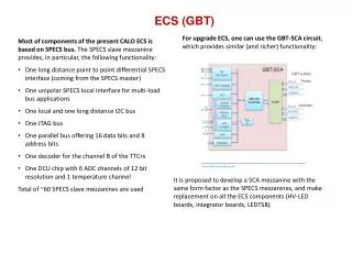
The GBT – SCA GBT-SCA Main specs: • Dedicated to slow control functions • Interfaces with the GBTX using a dedicated E-link port • Communicates with the control room using a protocol carried (transparently) by the GBT • Implements multiple protocol busses and functions: • I2C, JTAG, Single-wire, parallel-port, etc… • Implements environment monitoring functions: • Temperature sensing • Multi-channel ADC • Multi-channel DAC Engineers: • Alessandro Gabrielli – INFN, Italy • Kostas Kloukinas – CERN, Switzerland • Sandro Bonacini – CERN, Switzerland • Alessandro Marchioro – CERN, Switzerland • Filipe Sousa – CERN, Switzerland Status • Specification work undergoing: • 1st Draft already available • RTL design undergoing • 10-bit ADC prototype: • Submitted for fabrication in April 2010 • Received from the foundry in February 2011 • Test results expected soon • Fabrication of the final version in 2011 Paulo.Moreira@cern.ch
The GBT - SerDes The GBT – SerDes is a demonstrator for: • The Serializer/De-serializer critical circuits: • Phase-Locked Loops • Frequency dividers • Line driver/receiver • Constant-latency barrel shifter • Phase shifter • Target data rate: 4.8 Gb/s • The chip was packaged in a custom flip-chip BGA package Engineers: • Ozgur Cobanoglu - CERN, Switzerland • Federico Faccio - CERN, Switzerland • Rui Francisco – CERN, Switzerland • Ping Gui – SMU, USA • Alessandro Marchioro - CERN, Switzerland • Paulo Moreira - CERN, Switzerland • Christian Paillard - CERN, Switzerland • Ken Wyllie - CERN, Switzerland Status: • Chip is currently under testing Paulo.Moreira@cern.ch
Data path Clocks Control bus The GBT – SerDes Architecture dOut [29:0] DES Frame Aligner Switch FECDecoder Switch De-scrambler Header decoder Switch Parallel Out/ BERT rxDataValid 120 120 120 120 120 120 Serialinput rxClock40 rxClock160 ClkOut3 Phase Shifter ClkOut2 120 ClkOut1 120 120 ClkOut0 Clock Generator RX: 40 MHz & 160 MHz Clockreference rxRdy Control Logic txRdy TX: 40 MHz & 160 MHz I2C JTAG AUX[n:0] RST dIn [29:0] SER Switch FECEncoder Switch Scrambler Header encoder Switch Parallel In/ PRBS 120 120 120 120 120 Serial out txDataValid 120 txClock40 txClock160 Full custom PROMPT Power On RESET reset Paulo.Moreira@cern.ch
Ser & Des Serializer De-Serializer The receiver is fully functional but only up to ~3 Gb/s! Performance: Clock recovery operates up to 6 Gb/s Jitter: Recovered 40 MHz clock PRBS @ 4.8 Gb/s: Total jitter (1e-12): 63 ps Random jitter: 4.9 ps (rms) Deterministic jitter: 24 ps (pp) Periodic: RMS: 2 ps PP: 5 ps • The serializer if fully functional and fully complies with the specifications: Performance: • Data transmission: • No error observed • Jitter: • Total jitter (1e-12): 53 ps • Random jitter: 2.4 ps (rms) • Deterministic jitter: 19 ps • Data dependent: 4.8 ps • Periodic: • RMS: 4.6 ps • PP: 19.6 ps • Duty-cycle-distortion: 0.6 ps • Inter-symbol interference: 4.8 ps Paulo.Moreira@cern.ch
De-Serializer: Prime Suspects De-serializer timing Package signal integrity: A bad quality eye-diagram is observed at the chip input! Modeling of the package confirmed that the package is having a strong impact on signal integrity A new package is being designed and is now being manufactured • Testing and simulations have confirmed that the following functions perform correctly: • The clock recovery • The digital receiver functions: • Frame aligner • FEC decoder • De-scrambler • I/O parallel interface • The problem is confined to the serial-to-parallel conversion function: • The architecture is critically dependent on correct timing • The problem is now identified: • A timing problem exists on the distribution of the fast de-serializing clock • The future GBTX will use a intrinsically “timing robust architecture” to solve this problem. Eye – Diagram at 4.8 Gb/s Comparison: Measurement/Simulation Simulation with a SiWave model Measured at the termination Paulo.Moreira@cern.ch
Phase – Shifter Phase-Shifter: • Main features: • 8 – channels (3 in the GBT-SERDES prototype) • 1 PLL + Counter generates the three frequencies: 40 / 80 and 160 MHz • 1 DLL per channel • Mixed digital/analogue phase shifting technique: • Coarse de-skewing – Digital • Fine de-skewing – Analogue • Power consumption: • PLL: 42 mW (measured) • Channel: 16 mW/channel (measured) Engineers : • Ping Gui – SMU, USA • Tim Fedorov – SMU, USA • Paul Hartin – SMU, USA • Nataly Pico – SMU, USA • Bryan Yu – SMU, USA Status: • Fully functional • Fully meets the specs • One channel with timing problems butthe cause is clearly identified with trivialsolution • CK Period Jitter:s = 4.8 ps (pp = 29 ps) • Resolution:Dt = 48.83 ps • Differential Non-Linearity: • s = 4.7 ps (9.6% of Dt) • pp = 21.5 ps (44% of Dt) • Integral Non-Linearity: • s = 4.3 ps (8.7% of Dt) • pp = 21.9 ps (48.7% of Dt) Paulo.Moreira@cern.ch
The GBT Protocol on FPGAs • GBT-SERDES successfully implemented in FPGAs: • Scrambler/ Descrambler + Encoder/ Decoder + Serializer/CDR • FPGA Tested: • XILINX Virtex-5FXT and 6LXT • ALTERA Stratix II and IV GX • Optimization studies: • Optimization of use of resources (2009) • Low and “deterministic” latency (2010) • Firmware: • “Starter Kit” is available for download with various resources optimization schemes for • StratixIIGx and Virtex5FXT • Available soon for: • StratixIVGx and Virtex6LXT • Low latency • Engineers: • Sophie Baron – CERN, Switzerland • Jean-Pierre Cachemiche – CPPM, France • Csaba Soos – CERN, Switzerland • Steffen Muschter - Stockholm University • Users: • 30 registered users from all over the world (most users from collaborating institutes) • LHC experiments, but also CLIC, PANDA, GBT • Very active users are now part of the development team Xilinx - 4.8 Gb/s Altera + opto TRx - 4.8 Gb/s Paulo.Moreira@cern.ch
GBTX Block Diagram External clock reference FEModule Clock[7:0] E – Port Phase - Shifter CLK Reference/PLL E – Port FEModule E – Port E – Port DEC/DSCR CDR Phase – Aligners + Ser/Des for E – Ports 80, 160 and 320 Mb/s ports CLK Manager SCR/ENC SER E – Port FEModule E – Port E – Port One 80 Mb/s port Control Logic Configuration GBT – SCA JTAG I2C Slave I2C Master E – Port I2C (light) data JTAG Port I2C Port control clocks Paulo.Moreira@cern.ch
SEU tolerant GBTX – to – Frontend Communication • GBTX – to – Frontend interface: • Electrical links (e-link) • Bidirectional • Operate in: • Serial and Parallel Modes • Up to 40 active links • E-Link: • Three pairs: • DOUT: GBTX –to – Frontend • DIN: Frontend – to – GBTX • CLK: GBTX –to – Frontend • Programmable data rate: • Independently for up/down links • Independently in five groups(of up to 8 links each) • 80, 160 and 320 Mb/s • Lanes: • To achieve > 320 Mb/s • Two or more e-links can be grouped forming a “lane” • Slow data rate channel: • Fixed data rate: 80 Mb/s • General purpose data transmission • Compatible with GBT – SCA • Electrical standard: • SLVS electrical levels: • 100 W termination • 400 mV differential • 200 mV common mode • ILOAD = ±2 mA JEDEC standard, JESD8-13 Scalable Low-Voltage Signalling for 400 mV (SLVS-400) http://www.jedec.org/download/search/JESD8-13.pdf Paulo.Moreira@cern.ch
GBTX 8B/10B Transmitter Mode • In this mode: • 8B/10B encoding is used • No SEU protection • Only available in the simplex transmitter mode • Motivation: • Simplicity of the FPGA receiver • Significant reduction of the resources used by the GBT receiver in the FPGAs • Implementation: • A first special word is required for frame synchronization: • Comma character will be used • Idle/data frames: • Data frame (txDataValid = 1): One comma character followed by 11 8B/10B words • Idle frame (txDataValid = 0): To be specified! • The 12-word 8B/10B encoder will very likely require additional GBTX latency! • To reduce the package cost and the pin count some of the (normally) GBTX output ports will work as inputs • Bandwidth: • User bits: 88 (82 in the GBT protocol) • User data rate: 3.52 Gb/s (3.28 Gb/s in the GBT protocol) • 3.52 Gb/s vs 3.28 Gb/s → 7.4% increase only! 5 groups of 8 E-ports 1 group of 4 E-ports 8B/10B 8B/10B 8B/10B 8B/10B 8B/10B 8B/10B 8B/10B 8B/10B 8B/10B 8B/10B 8B/10B 8B/10B Comma character: indicates start of frame 88 user bits total → Data rate = 3.52 Gb/s (No commas allowed in the other positions) Paulo.Moreira@cern.ch
GBTX Chip and Package Size • Total pin count: 434 • Chip size: 5.5 × 5.5 = 30.25 mm2 • Fits a 21 × 21 pin Package • Approximate package size: • 1 mm pitch: 22 × 22 mm2 • 0.8 mm pitch: 18 × 18 mm2 Paulo.Moreira@cern.ch
GBTX Power Consumption Paulo.Moreira@cern.ch
Project Schedule Tasks remaining: • GBT – SerDes: • Understanding the receiver behaviour: • 3 Gb/s error free operation instead of4.8 Gb/s • SEU tests • GBTX: • Receiver rework • Power down functions (SER/CDR) • TX 8B/10B mode • Clock Manager • VXCO based PLL • 8 channel Phase-Shifter (only 3 on GBT - SerDes) • Implement the 8B/10B transmitter mode • E – Links • Bi-directional C4 pad • Serializers • Phase-Aligners • E-Ports: • Implement a bidirectional C4 pad with switchable termination resistor • Control Logic: • Watchdog and start-up state machines • IC channel logic • I2C master • Configuration logic: • Fuse bank • Chip assembly and verification • From industry: • BGA package (flip-chip) • 80 MHz crystal • Testing: • Test setup • Early behavioral model needed for test development • Software • Firmware • GBLD: • Reduce the area of the input protection diode • Improve the bandwidth and gain of the input stage • Design/choose a package with good thermal conductivity • Change I/O to 1.5V • GBTIA • Change pad ring, add average power detector and add squelch circuit • Migration from the LM to the DM technologies flavor • 2.5V Supply Project Schedule 2011 • SEU tests on GBT – SerDes • May • ASIC submissions: • GBLD: August • GBT – SCA: November • GBTIA: November • GBTX: November Paulo.Moreira@cern.ch

