Download
1 / 13
130 likes | 146 Views
Learn about the SVX4 chip, part of the SVX family of chips designed for CDF and D0 detectors. Discover its features, design process, and analog performance.

E N D
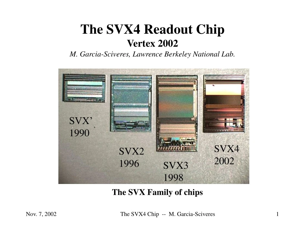
The SVX4 Readout ChipVertex 2002M. Garcia-Sciveres, Lawrence Berkeley National Lab. SVX’ 1990 SVX4 2002 SVX2 1996 SVX3 1998 The SVX Family of chips The SVX4 Chip -- M. Garcia-Sciveres
Credits & History • Design Team: • LBNL:Brad Krieger (lead designer), Jean-Pierre Walder (ADC), Henrik von der Lippe (I/O pads), Emanuelle Mandelli (full chip simulation) • FNAL:Tom Zimmerman (preamp & pipeline), Jim Hoff (pipeline logic) • U. of Padova:Stefania Alfonsi (FIFO) • Timeline • July 2000: First SVX4 proposal meeting following studies at LBNL • May 2001: Common CDF/D0 specifications supplied to designers. Preliminary design review. • October 2001: Final Design Review • April 2002: Design submitted for fabrication • June 10, 2002: Wafers delivered to FNAL • June 12, 2002: First chip tested at LBNL, basic functionality verified. The SVX4 Chip -- M. Garcia-Sciveres
Why SVX4? • Present CDF and D0 detectors not expected to survive beyond 4-6 fb-1 • Noise increase in SVX3 and SVX2 chips is important limitation on lifetime • Not possible to re-order existing chips to build new detectors • Take advantage of new Quarter Micron technology and work done for LHC experiments. • Functionally, SVX4 SVX3 + additional interface logic to make it optionally heave like SVX2 chip. ~ = The SVX4 Chip -- M. Garcia-Sciveres
Review of SVX3(presented at Vertex 1998) ADC • Low resistivity substrate exploited for ground distribution and digital/analog isolation • Real time pedestal subtraction built into ADC 8 Charge sensitive amplifier with adjustable risetime Dual-ported analog pipeline for dead-timeless operation Wilkinson type ADC 128 channels in parallel Zero-suppressed readout on 8-bit parallel bus The SVX4 Chip -- M. Garcia-Sciveres
SXV4 features • Use same floor plan as SVX3 • Most analog circuits redesigned at schematic level- full custom layout • Digital circuits made using library parts from rad-hard library developed for ATLAS pixel chip, based on RAL quarter micron library. • Use low resistivity substrate as in SVX3 • Add on-chip decoupling capacitance • Design relies heavily on fantastic accuracy of high volume commercial process simulation tools – this is THE biggest change relative to traditional rad-hard electronics. The SVX4 Chip -- M. Garcia-Sciveres
Results • Full SVX4 chip was simulated before submission. The problem is no longer “can you simulate it” but rather “what to simulate”. • First full size chip fabricated is essentially a usable chip:The number of changes needed for the next SVX4 submission is less than the number of changed made for the SVX3 production run. • The things that need to be fixed were not caught by the simulation because the right things were not simulated. • Every item could be simulated after the fact, including a very subtle ADC effect (shown later). • Radiation tolerance to spare. SEU x-section lower than SVX3- same register cells as ATLAS but 100 times fewer of them. The SVX4 Chip -- M. Garcia-Sciveres
Analog performance 100ns integration time, 70ns 0-90% rise time, 290uA/channel preamp current The SVX4 Chip -- M. Garcia-Sciveres
Zero-Suppressed Data Out “FIFO” • SVX3 “FIFO” is full custom, dynamic logic circuit with asynchronous collapse to achieve zero suppression. • This was the only way to do it fast enough in 0.8mm. • 0.25mm is SO MUCH faster that we could instead use a fully synchronous, automatic place and routed VHDL circuit with no collapse phase- zero suppression happens in real time during readout. • At design readout speed if 53MHz it works exactly except for some special low occupancy hit patterns in which case a single extra readout clock is used. This OK for us. The SVX4 Chip -- M. Garcia-Sciveres
Full chip Simulation • >300K transistors • TIME-MILL program with some tricks • Save DC points of programmable registers • About 1hr per ms The SVX4 Chip -- M. Garcia-Sciveres
ADC Comparator channel-to-channel scatter Measurement: Each line is a different comparator bias current Less bias ADC counts (pedestal) More bias Channel number • Pedestal shifts but gain is the same for all traces The SVX4 Chip -- M. Garcia-Sciveres
ADC scatter cause • All comparators identical at schematic and layout levels. • Quarter micron circuits it turns out are particularly sensitive to tiny threshold mismatch in “matched” (at layout level) transistors. – This is NOT the same thing as lot-to-lot global variations or “corners” • TSMC in fact provides data on this type of mismatch for every transistor parameter (for IBM data comes from a thesis) • With these data one can run a Monte Carlo circuit simulation were the parameters are wiggled for selected transistors. • We wiggled other parameters, not just Vth, but found that Vth is the only one that matters. • Interestingly the ATLAS FE chip was also bitten by this bug, which led to a higher than desired threshold dispersion in current prototype. We copied the MC simulation idea from them. The SVX4 Chip -- M. Garcia-Sciveres
MC Simulation of Channel-to-Channel Variations ADC counts Bias current Measured SPREAD Measured DELAY Simulated, 4 transistor MC Simulated, 4 transistor MC Simulated, all transistor MC Simulated, all transistor MC The SVX4 Chip -- M. Garcia-Sciveres
Conclusion • SVX3 circuit was converted to .25mm with some enhancements in a little over 1 year. • SVX4 significantly outperforms SVX3. • Full chip prototype in hand 2 years after first we though of doing it is already closer to a production chip than the final SVX3 prototype was. • Really a new (to us) way to design ICs. Use state of the art industry tools for high volume process. Full chip simulation leading to very high confidence submission. The SVX4 Chip -- M. Garcia-Sciveres