Download
1 / 26
270 likes | 458 Views
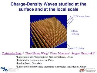
Charge- Density Waves studied at the surface and at the local scale. CDW wave fronts. NbSe 3 T=83 K. quasi-1D chains. Christophe Brun 1,2 Zhao-Zhong Wang 1 Pierre Monceau 3 Serguei Brazovskii 4. 1 Laboratoire de Photonique et Nanostructures, Orsay

E N D
Charge-DensityWavesstudiedat the surface and at the local scale CDW wave fronts NbSe3 T=83 K quasi-1D chains Christophe Brun1,2 Zhao-Zhong Wang1 Pierre Monceau3 Serguei Brazovskii4 1Laboratoire de Photonique et Nanostructures, Orsay 2Institut des Nanosciences de Paris 3Institut Néel, Grenoble 4Laboratoire de physique théorique et modèles statistiques, Orsay
Motivation Electronicpropertiesat the surface vs bulkproperties 48 Fe atoms on Cu(111) 2DEG confinement [1] [1] Crommie, Lutz, Eigler, Science 262, 218 (1993)
Motivation Electronicpropertiesat the surface vs bulkproperties 48 Fe atoms on Cu(111) 2D-CDW: 1T-TaSe2 Increased U/W Mott transition at the surface [2] 2DEG confinement [1] [1] Crommie, Lutz, Eigler, Science 262, 218 (1993) [2] Perfetti, Georges, Florens, Biermann, Mitrovic, Berger, Höchst, Grioni, PRL 90, 166401 (2003)
Motivation Electronicpropertiesat the surface vs bulkproperties 1D-CDW: Rb0.3MoO3 48 Fe atoms on Cu(111) 2D-CDW: 1T-TaSe2 2D-FFT qcdw 2b* 10 nm 2(a+2c)* Increased U/W qb*=0.30 b*≠ 0.25 b* bulk value Spatially inhomogeneous CDW wave vector [3] Mott transition at the surface [2] 2DEG confinement [1] [1] Crommie, Lutz, Eigler, Science 262, 218 (1993) [2] Perfetti, Georges, Florens, Biermann, Mitrovic, Berger, Höchst, Grioni, PRL 90, 166401 (2003) [3] Machado-Charry, Ordejon, Canadell,Brun, Wang, PRB 74, 155123 (2006)
Motivation Electronicpropertiesat the surface vs bulkproperties 26 nm LaAlO3/SrTiO3 SrTiO3 upon UV light 480J/cm2 55 eV Interface 2DEG [1] Surface 2DEG [2] [1] Ohtomo, Hwang, Nature 427, 423 (2004) [2] Meevasana, et al. Nature Mat. 10, 114 (2011)
Outline • Experimental set-up: UHV-LT-STM • Characterization of the two CDW phases at (100) surface of NbSe3 • Surface transition for q2 CDW (Tcsurface > Tcbulk) • Evidence for microscopic amplitude solitons and Friedel oscillations
Experimental STM Set-up: UHV - 5 K based on an Omicron STM 3.0 10-11 mbar
Scanning Tunneling Microscopy/Spectroscopy Sample Tip Vacuum Finite T: broadening ~ 3.2kBT
NbSe3 basic properties b b Δz Se atoms ~ 1.5Å b=3.5Å • b= 600 .cm (300K) ) b/ c=300 et b/ a=1200 • 144K: CDW transition. chains III. 21 ~ 200-300meV. q1= 0.241b* • 59K: CDW transition. chains I. 22 ~ 70-130meV. q2= 0.5a* + 0.259b* + 0.5c* • Metallicatlow T c=15.6Å I II III I II III ( b,c ) plane
300Kcleavage in UHV Prodan et al., PRB54, 10370(1996) Previous STM measurements on NbSe3
77Kin liquid N2. CDW ? Slough et al., PRB 39, 5496 (1991) 300Kcleavage in UHV Prodan et al., PRB54, 10370(1996) Previous STM measurements on NbSe3
77Kin liquid N2. CDW ? Slough et al., PRB 39, 5496 (1991) 300Kcleavage in UHV Prodan et al., PRB54, 10370(1996) 4Kin liquid He. Observed CDWs Dai et al., PRL 66, 1318 (1992) Previous STM measurements on NbSe3
77Kin liquid N2. CDW ? Slough et al., PRB 39, 5496 (1991) 300Kcleavage in UHV Prodan et al., PRB54, 10370(1996) 4Kin liquid He. Observed CDWs Dai et al., PRL 66, 1318 (1992) Previous STM measurements on NbSe3 • Three types of chains observed • q1 and q2 CDWs observed only at 4 K • Contrast (LDOS) determined by Se atoms [1] • No measurements on UHV cleaved samples at low temperature [1] Ren and Wangbo, PRB 46, 4917 (1992)
L ~ 0.5mm l ~ 30mm Remaining NbSe3 floating filaments Ø = 250 m Sample preparation • NbSe3 : whisker-like sample • In-situ cleavageunder UHV at 300K l ~ 15mm Synthesis: H. Berger (EPFL - Lausanne)
q1 CDW and atomic lattice Tc1=144K, Tc2=59K 78K V=+100mV I=1nA Z~0.3ÅZCDW ~ 0.15Å 20x20nm2 Raw data image
b=3.5Å c=15.6Å I II III I II III ( b,c ) plane q1 CDW and atomic lattice Identification of chains III: whereq1 CDW is the mostdevelopped 2D Fourier Transform • q1 = 0.24b*in agreement withbulk value • Chains II are alsoweaklymodulated by q1 CDW
q1 and q2 CDW with the atomic lattice Tc1=144K, Tc2=59K 5K V=+200mV I=0.15nA Z~0.3ÅZCDW ~ 0.15Å 25x25nm2 Raw data image
q1 and q2 CDW with the atomic lattice Identification of chains I: whereq1 CDW is the mostdevelopped • q1 = 0.24b*q2 = 0.26b*+ 0.5c*in agreement withbulk values • Chains II and III are alsomodulated by q2 CDW Brun, Wang and Monceau, PRB 80, 045423 (2009)
Surface transition for q2 CDW 100 x 100 nm2
Surface transition for q2 CDW Vbias = -0.3 eV STM, x-rays, CDW-CDW tunneling • Evidence for a surface transition at 70-75 K > Tcbulk = 59 K Fleming, Moncton, and McWhan, PRB 18, 5560 (1978) O’Neill , Slot, Thorne, Van der Zant, PRL 96, 096402 (2006)
Tcbulk Tcsurf 3D ordering 59-63K [1] Surface transition for q2 CDW Inverse correlationlengthsextractedfrom profiles in FT plane • 2D regime – CDW at surface decoupled from bulk : 63 - 88K • BKT with TBKT ~ 88 K [1] Rouzière, Ravy, Pouget, Thorne, Solid State Commun 97, 1073 (1996) Brun, Wang, Monceau, Brazovskii, PRL 104, 256403 (2010)
Plausible mechanism of surface Tc enhancement • Role of phonons propagating in the surface plane [1] • Atom displacements normal to the surface are larger than in the bulk (absence of restoring force + relaxation) E(surface_transverse phonon modes) < E(bulk_transverse phonon modes) e-ph coupling constant λsurface > λbulk Tc_surface ~ W.exp(-1/ λ surface >) > Tc_bulk 20% increase in Tc results from 4% change in λ • q2 superlattice atom displacement possess components along a*[2] [1] Brown, Fradkin, Kivelson, PRB B 71, 224512 (2005) [2] Van Smaalen et al. PRB B 45, 3103 (1992)
Other surface transitions • NiO(100) – helium scattering [1] • TNéel_surface > TNéel_bulk • NbSe2 – Inelastic grazing x-rax diffraction [2] • Tc_surface > Tc_bulk and softer surface phonons • cuprate Ca2-xNaxCuO2Cl2 – STS [3] • Surface charge ordering – no bulk counter part [1] Marynowski, Franzen, El-Batatouny, Staemmler PRB 60, 6053 (1999) [2] Murphy et al. Physica B 336, 103 (2003); PRL 95, 256104 (2005) [3] Hanaguri et al. Nature, 430, 1001 (2004)
Electronic bands measured by ARPES 300K Bandwidth ~ 0.3 eV Shäfer, Rotenberg, Kevan, Blaha, Claessen, Thorne, PRL 87, 6053 (2001)
Conclusion • NbSe3 surface plane : q1 and q2 in very good agreement with bulk values • Surface transition at 70-75K above the 59K bulk Tc • 2D BKT phase up to 88K • Observation of microscopic amplitude solitons and Friedel oscillations • Further quantitative modelling needed – extension of Tütto-Zawadowskii Acknowledgements H. Berger, E. Machado, P. Ordejon, E. Canadell, S. Ravy, J.-P. Pouget, S. Van Smaalen, A. Ayari, J-C. Girard and C. David