Download
1 / 26
280 likes | 627 Views
BULK Si (100) VALENCE BAND STRUCTURE UNDER STRAIN. Sagar Suthram Computational Nanoelectronics Class Project - 2006. Outline. Brief history of MOSFET scaling and need for Strained Silicon. Understanding Strain. Si valence band structure calculation using k.p method.

E N D
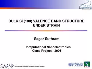
BULK Si (100) VALENCE BAND STRUCTURE UNDER STRAIN Sagar Suthram Computational Nanoelectronics Class Project - 2006
Outline • Brief history of MOSFET scaling and need for Strained Silicon. • Understanding Strain. • Si valence band structure calculation using k.p method. • Si valence band structure calculation using tight binding method. • Strain effects on Si valence and conduction band – qualitative picture. • Summary
MOSFET Scaling History • Si MOSFET first demonstrated in SSDRC in 1960. • Improved dramatically due to gate length scaling driven by • Increased density and speed • Lower costs • Power improvements • Semiconductor industry scaled the MOSFET channels based on Moore’s law (1965). Simple geometric scaling followed. • Constant field scaling introduced by Dennard et. al. (1974).
MOSFET Scaling History • Constant field scaling too restrictive • Subthreshold nonscaling • Power-supply voltage not scaled proportional to channel length • Generalized scaling is preferable which allows oxide field to increase • Shape of 2-D electric field pattern preserved (channel doping engineering) • Short channel effects do not become worse
MOSFET Scaling Limits • But conventional planar bulk MOSFET channel length scaling is slowing • Increased off-state leakage • Increased off-state power consumption • Degraded carrier mobility due to very high vertical fields (thin oxides <2nm) • Lithographic limitations • Little improvement in switching performance • Inability to scale supply voltage and oxide thickness
Continued Transistor Scaling • “No exponential is forever” – Gordon Moore • But present scaling limits for Si MOSFET are caused by materials and device structure and are not hard quantum limits • Continued scaling requires new materials and device structures • High –K dielectrics • Strained Si • Novel channel materials (Ge, III-V semiconductors) • Non classical CMOS devices (FinFETs etc.)
Strained Silicon • Strained Silicon has been adopted in all advanced logic technologies • Scalable to future generations • Easily incorporated in existing processes • Enhances performance even in the ballistic regime due to effective mass reduction 90nm INTEL Technology node transistor with process induced uniaxial stress [Thompson 04]
How is strain added to silicon ? • Uniaxial stress is induced in the following ways • SiGe source-drain for PMOS • Tensile nitride capping layer for NMOS
How is strain added to silicon ? Biaxial stress is induced by epitaxialy growing a silicon layer on relaxed SiGe. The lattice mismatch induces biaxial tensile stress in the silicon layer.
Outline • Brief history of MOSFET scaling and need for Strained Silicon. • Understanding Strain. • Si valence band structure calculation using k.p method. • Si valence band structure calculation using tight binding method. • Strain effects on Si valence and conduction band – qualitative picture. • Summary
Understanding Strain Stress (s) : Strain (e) :
Understanding Strain Elastic Stiffness Coefficients Elastic Compliance Coefficients
Outline • Brief history of MOSFET scaling and need for Strained Silicon. • Understanding Strain. • Si valence band structure calculation using k.p method. • Si valence band structure calculation using tight binding method. • Strain effects on Si valence and conduction band – qualitative picture. • Summary
Silicon valence band using k.p The form of the Schrodinger equation when written in terms of unk(r) near a particular point k0 of interest.
Silicon valence band using k.p • Luttinger-Kohn’s model: k.p method for degenerate bands • Mainly for silicon valence bands • Consider the heavy hole, light hole and split-off bands as class A and rest of the bands as class B • Use 2nd order degenerate perturbation theory
Outline • Brief history of MOSFET scaling and need for Strained Silicon. • Understanding Strain. • Si valence band structure calculation using k.p method. • Si valence band structure calculation using tight binding method. • Strain effects on Si valence and conduction band – qualitative picture. • Summary
Silicon Valence band using tight-binding method pz px py • sp3s* tight binding picture used • 20x20 Hamiltonian including spin-orbit interaction considered • Silicon valence band predominantly composed of p-bonding states which are degenerate at the G point
Outline • Brief history of MOSFET scaling and need for Strained Silicon. • Understanding Strain. • Si valence band structure calculation using k.p method. • Si valence band structure calculation using tight binding method. • Strain effects on Si valence and conduction band – qualitative picture. • Summary
Strain effects on silicon valence band • Splits the degeneracy of the valence band at the G point • The bands are no longer just HH or LH due to the strong coupling between the two, but either HH-like or LH-like • Biaxial stress does not warp the bands much due to the presence of only a hydrostatic component in the strain matrix which maintains the crystal symmetry. • Uniaxial stress warps the bands causing a reduction in the effective mass due to the presence of a shear term which destroys the crystal symmetry
Summary • k.p method is emperically based and treats the band structure with precision • k.p is useful for calculating band structure only for k values close to the band edge which is generally the region of interest • Tight-binding on the other hand considers the microscopic interatomic interactions and hence gives a good physical insight into the strain effects on the band structure • We see differences in the exact band structures computed by the two methods but they show similar trends under the application of strain • Computing more accurate band structures with the tight-binding method involves consideration of up to 10 orbitals (sp3d5s*) along with spin which gets very complicated when the strain effect is added Thank You