Download
1 / 34
340 likes | 355 Views
This document provides an overview of the Calorimeter Digitizer System, including the system block diagram, ADC choice, and data flow for the FPGA and trigger. It also covers the trigger daughter card and off-detector ADC system.

E N D
Calorimeter Digitizer System • Overview • System block diagram • ADC choice • Digitizer Board flow • FPGA data flow • Trigger data flow • Trigger daughter card.
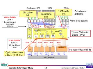
Calorimeter Digitizer system overview • Off detector ADC system for both EM and Hadronic calorimeter. • Received the amplified signal from on-detector amplify through cables • Digitize the signal at 6x beam crossing rate, ~ 60 MHz, with 14 bits ADC • Offset the baseline to use most of the ADC range. • Provide at least 40 beam crossing of data buffers to cover L1 trigger latency • Provide Level 1 trigger primitives. • Minimum 4 Level 1 events buffer. • Maximum 31 ADC samples per channel per events, 16 samples planned. • 15 KHz Level 1 trigger rate (16 Samples/channel/Event). • Send Level 1 trigger events to the DAQ system. • 24576 EMCAL channel, 1536 HCAL Channel. Calorimeter Electronics Digitizer System Design Review
The Subsystem Technical Overview Crate based system. Signals are cable from the on-detector electronics. Digitized with 14 bit ADC. Receive timing information the SPHENIX Granule Timing Module (GTM) Generate L1 trigger primitives Receive L1 trigger and send out L1 triggered event data to Data Collection Module II (DCMII). Provide buffer for both the 40 beam crossing L1 delay buffer and 4 L1 triggered events crate Clock are fanout point to point through the backplane Trigger out Trigger out Slow control/readback bus, L0, L1 trigger Token passing dataway Token passing dataway XMIT Controller ADC ADC 3 ADC XMIT (rack based) detector clockmaster 3Gbit/sec optical link 1.6Gbit/sec optical link Slow control/readback Beam clock, L0, L1 trigger DCM II JSEB II GTM SPHENIX DAQ System PC Calorimeter Electronics Digitizer System Design Review
The Choice of ADC Analog device AD9249 16 channel 14 bits ADC. Maximum sampling rate 65 MHz SNR 75db 1.8v technology. 58mw per channel at 65 MHz -> 1 W per chip. 144 pins package. 1cm X 1cm BGA pipeline latency 16 clocks. Analog Device AD9257 8 channel 14 bits ADC Maximum sampling rate 65 MHz SNR 75.5 db 1.8v technology. 55mw per channel at 65 MHz 65 pins LFCSP package. 0.9mm by 0.9mm. pipeline latency 16 clocks. Texas instrument ADS5294 8 channel 14 bits ADC. Maximum sampling rate 80 MHz SNR 75.5db 1.8v technology. Per channel 58mw at 50 MHz, 77mw at 80 MHz. 1-wire only interface only for below 50 MHz sampling 80 pins QFP package. 12mm by 12mm included digital processing block ( only after digitization) pipeline latency 11 clocks for 1 wire interface. Linear Technology LTM9008-14 8 channel 14 bits ADC. Maximum sampling rate 65MHz SNR 73 db 1.8v technology. Per channel 88mw at 65 MHz. 140 pins BGA. 11.25mm X 9mm pipeline latency 6 clocks. • The limit of ADC LVDS serializer • seems to be less than 1Gbits/sec • 65 MHZ ADC • The FPGA does not have 128 LVDS • De-serializer 1 LVDS output • per ADC channel • JSED204B’s ADC need the transceiver to receive data • Limits number of ADC can be connected to the reasonable price FPGA Calorimeter Electronics Digitizer System Design Review
sPHENIX ADC Module Block Diagram RHIC beam clock 9.6MHz +4V, -3.5V, +2.5V Power 7X ADC clock Analog Device AD9257 8 channel 14bits 65 MHz ADC +- 3.5V, -2.5V Differential receiver power +1.8V analog ADC power +1.8V digital ADC power F R A M E ALTERA Arria V GX BB1D4F35 1152 pins FPGA 6x beam clock Beam phase, init, L1 Serialized ADC DATA Differential receiver De-serializer D P U two transceivers 2 mm Hard Metric Token Passing Data 5 L1 Accepted Event buffer L1 Delay Buffer Serialized Token Passing Clock Fanout 64 channel ADC board 6 X beam clock Serial command two transceivers 2 mm Hard Metric L1 trigger primitives transceiver out command/ offline data read De-serializer F R A M E Differential receiver Serialized ADC DATA Bused command Serial data 3.3V LDO 3.3V LDO Analog Device AD9257 8 channel 14 bits 65 MHz ADC DC/DC switch regulator 4V +12V Power DC/DC switch regulator 2.5V FPGA I/O 7X ADC clock 1.5V LDO 1.1V core Calorimeter Electronics Digitizer System Design Review
Sphenix 64 channel ADC Data Flow Diagram BC & L1 event numbers Header 512X16 Header 8 x 32 Beam clock number 6x RHIC clock 6x RHIC clock L1 trigger 8b/10b encoding Serialized data from down Stream board 14 bits ADC serialized data 840 Mbits/sec LVDS L1 Delay memory 512X128 8 events buffer 256 X 1024 FIFO 2048 * 34 bits (first, data, Last) Alignment 16bits FIFO Gbits receiver Input control De-serialize /alignment 1-8 16bits FIFO Gbits receiver Fake data 512X16 1-64 channels wadd Token in radd = wadd - delay 8b/10b encoding Serialized data Gbits transmitter Link control L1 trigger Primitives generators Token out 120 MHz Reference clock 80 MHz Reference clock Write address 3 bits events, 5 bits samples Gbits transmitter write = valid & token Read = !empty read address 3 bits events, 5 bits samples LVDS repeater Slow control readback backplane Optical transceiver Lemo out Daughter card Calorimeter Electronics Digitizer System Design Review
Cal trigger primitive Generator (preliminary) 6X BC clock 120 MHz clock 12X BC Clock delay +1 +2 + 1 BC + 2 12X +1 4 bits trigger phase only use upper 8 bits Dual port memory Baseline subtraction Lookup memory (1024X10) Choose one of the of of the 12X BC clock phas for trigger primitive 10 bits 2X2 SUM (12 bits output) MUX 128 bits To 8 16 bits 10X16 bits FIFO Transceiver IP Read Address (upper 10 bits) Load lookup Memory from Slow control Read address = write address -delay Sub = ADC – ADCpre If (adcpre> adc) sub=0 64 channels 16 2X2 8 bits sum Delay a parameter Probably has 2 clocks offset Monitor Delay dual port memory 5 events buffer To controller readout Delay and # of Sample adjustable L1 trigger Calorimeter Electronics Digitizer System Design Review
Trigger daughter plug in from the back with 2 outputs, 1 optical transceiver, 1 lemo output. backplane Optical transmitter output ARRIA 5 FPGA LVDS buffer Lemo out Trigger daughter card 3.3v Calorimeter Electronics Digitizer System Design Review
Calorimeter Local Level 1 Trigger • A difficult project • Lots of data with limit amount of resources • Organize the data flow • Understand the Inputs • Lots of inputs few outputs • What we try to do • Calorimeter Sum • Deal with geometry.. Over lapping sum neighbor problem • Clocks and L0 timing • Go through proposed solution as an example • Alternative hardware choices • What we done so far • Next steps
Inputs • Total emcal channel = 96*256 = 24576. • Phi and eta coverage is 0.025 *0.025 • HCAL has 24576/16 = 1536 channel (outer only) • Phi and eta coverage is 0.1*0.1 after 2X2 sum => 0.2 *0.2 coverage • 2x2 sum are done in FEM. Each sum has 8 bits. • Finest element we could send out in the FEM, constrained by the bandwidth of the system. • So we have 384 L1 primitives fibers from EMCAL and 24 from HCAL. • If we can not bring all fibers into one FPGA, we are dealing with processing data in subset of the detectors.
Physics goals • Hadronic jets • SUM over EMCAL + Hadronic towers • With 0.2 eta X 0.2 phi tower overlapping 2x2 sum. • Threshold apply over the 2x2 sum. Isolation cuts. • Pair trigger • With EMCAL 4x4 overlapping sum • SUM threshold applied, isolation cut applied • 10 bits energy (??) with both eta and phi angle • 3 bits eta and phi address will be enough to reconstruct the mass. • May be a look up table??
4x4 sum require data from neighbor 2x2 cells • Simple isolation cuts will required data from neighbor 4x4 sum. • Overlapped 4x4 sum mean we have as many 4x4 sum as input 2x2 sum . • For example as • 4x4 matrix of 2x2 sum will require data from 2 top rows, 2 left columns, 1 bottom rows and 1 right columns. • Bring in more data from neighbor region. • Constrains building “trigger processing blocks” either in complete phi or complete eta. • So we only have deal cross stitching from two edge only • Trigger block should at least cover 8 2x2 width • Limit the bring the neighbor data to less than 3/8 of input bandwidth. 4x4 sum (2x2 of <2x2> sum) 05 05 15 25 35 45 55 4x4 overlapped sum 04 14 24 34 44 54 03 13 23 33 43 53 02 12 22 32 42 52 01 11 21 31 41 51 Simple Isolation cut 00 10 20 30 40 50 >= > > >= 41 > >= >= >
Data division • The EMCAL data have 256 channel phi and 96 channels in eta. • Assume • Each fiber cover 64 channel in square form (8x8) for each cable mapping • 2 layers of 8x8 channels • If complete phi coverage 64 fibers, For complete eta coverage 24 fibers per trigger processing blocks. • Plus sending and receiving of cross stitching fibers from neighbor region. Ignore end of the detector effect.
Clock Domain • The collider beam interaction is driven by the RHIC beam clock, ~9.6 MHz • The calorimeter digitizer is driven by 6X beam clock. • The L0 timing signal, like RESET, INIT, TEST, RUN etc., carries action associate with beam clock. • The L1 trigger primitives optical transmitter is driven by 120 MHz crystal clock • For the clock stability. Use local crystal… • The L1 trigger block needs • 1) beam clock is needed to clock the collision data • 2) reference clock is needed to receive the data. • 3) FPGA operation could be drive by multiple of the reference clock. • Simplify the optical interface coupling… • Per reference frequency, several possible optical speed can be achieved.
Data input alignment with data merger block diagram Fake data injector Restore data to 16 2x2 sums Delay memory Alignment memory optical receiver unpacker Data collector Optical transmitter Data to Overlapped region Delay memory Restore data to 16 2x2 sums Alignment memory optical receiver unpacker Restore data sums optical receiver unpacker Data from Overlapped region slow control data readback sPHENIX internal review
Proposed system • Using existing calorimeter digitizer system infrastructure • Beam clock distribution • Slow control/offline read back system • Power distribution • 2 sets of 2 12V 50A power bug ensure enough DC power distribution. • Use only every other slots • Mechanical support
SPHENIX calorimeter Level 1 Trigger Conceptual design Borrow Calorimeter Digitizer infrastructure. Receive digitizer trigger primitives Provide cross stitching between tiles. Generate trigger primitives for global level 1 trigger Boards consists of two building blocks Each block has 36 optical receivers and 12 optical transmitter Altera Arria 10 20nm FPGA as the computing engine 1517 pin package. 0.95V core. Optical speed up to 6.5Gbps 570K logic element 600K, 900K, 1150K The cost should be around $1K-$2K per FPGA. Need to be reconfirmed. Trans- mitter R E C E I V E R 6A, 0.9V 2A each, 2.5V & 3.3V 4A, 1.8V 4A, 0.95V 4A, 1.8V 12V in
EMCAL Section (1) • L1 trigger Arria 10 GX block. • Assume we will do the trigger data along the eta direction. • 24 fibers will cover 96 channel in eta and 16 channel in phi direction. • Need 48 2x2 sum from the bottom block and 2 set of 48 sums from the top block. • The fundamental is 48 8 bits data. 24 16 bits data + 1 header + 1 beam clock + 1 space 27 data words bandwidth need to be at least 5.4 Gbits • The same thing hold true to copy data over to neighbors block. • This will call for 3 transmitters and 3 receivers for cross stitching • Or more lower bandwidth with more fibers.
EMCAL Section (2) • Need to do non-overlapping sum for Hadronic jets • Mapping is not uniform in eta and uniform in phi. • For bandwidth calculation use 8x8 non-overlapping which over 0.2 in phi. • Trigger block holds 24*16 2x2 sums => 384 2x2 sums => 24 8x8 sum. • This is about the same as single cross stitching data bandwidth requirement • 1 transmitter required. • For pair trigger, • set threshold on overlapping 4x4 sum. • Maximum 4 peak outputs. 6 bits address (eta, phi), 10 bits energy • This will require 1 transmitter.
Pair Trigger 16 inputs From EMCAL Shower max Jet Trigger HCAL Level 1 Trigger primitives concentrator 24 fibers Outer HCAL 16 inputs From EMCAL 8X8 sum 8 fibers output 24 fibers inner HCAL 8 inputs From HCAL 2x2 sum 0.2X0.2 eta and phi
FPGA Resource Usage • use example like proposed system • It deal with 96 channel in phi and 16 channel in phi 384 2x2 sum and generate equal amount 4x4 overlapped sum • Assume each of the sum has 10 bits. • This imply ~400 *2 *10 = 8K registers are needed per pipeline stage. • Assume we have 20 pipeline stages 160K. • This is not memory buffer intensive operation. • The FPGA logic cell size more or less match with number of optical transceivers • Comes with small feature, 20nm, 16nm, 14nm…
Alternative choice • Possible choice • Commercial solution –Hitech • ATLAS gFEX (Global Feature Extractor) board • ATLAS FELIX board • Questions to be asked • Does it meets the minimum choice ?? • Is it practical ??? • What are system design for?? Can it adapted for sphenix trigger?? • Can we handle it?? • The complexity of the system?? The infrastructure to operate it?? Man power to deal with it??
HiTechGlobal provide boards that similar to the ALTERA or XILINX evaluation board Have some boards with optical interface with CXP, QSFP etc. Optical FPGA interface tend to one side of FPGA. CXP has 12 port transceiver. QSFP(4 SFP) really for higher optical speed than 10 Gbits/sec than channel count. It is does not offer number of ports we are looking for.. FELIX is far better choice than Hitech if we are going through PCIE environment QSFP CXP
ATLAS/FELIX BNL-711 PCIe Card Credit: Kai Chen (BNL), https://indico.bnl.gov/conferenceDisplay.py?confId=2653 • BNL-711 Board chosen for ATLAS FELIX project, and used in ATLAS phase I upgrade, which is projected to complete before sPHENIX. • Readout for ATLAS Phase-I sub-system of Liquid Argon Calorimeter, Level-1 calorimeter trigger, New small wheel of the muon spectrometer MAPS workfest
ATLAS/FELIX BNL-711 PCIe Card Credit: Kai Chen (BNL), https://indico.bnl.gov/conferenceDisplay.py?confId=2653 • Main features for FELIX PCIe Card • Design: BNL/Omega group, Layout: BNL/Instrumentation, multiple users. • A large KintexUltrascale FPGA, 1.5 M LC • 48 bi-directional GBT link, PCIex16 Gen3, 101 Gbps demonstrated • 2x DDR4 memory slots (v1.0, v1.5), removed v2.0 • TTC-timing input (v1.0, v1.5), allow timing mezzanine card (v2.0) – provide help design sPHENIX GTM mezzanine card • Current version: v1.5 prototype, can be ordered • Next version: v2.0 pre-production, design starts now, expect available Oct 2017 • BNL/Omega group, Local expert expressed willing for helpus to adapt FELIX in sPHENIX • Boards for initial evaluation test, support firmware software development, timing mezzanine card design • The team is also help in possible use of FELIX card in protoDune. • The FELIX team is open for inputs in guiding the design to be more generic to various users. FELIX v1.5 Card in server, BNL ATLAS Group MAPS workfest
Why not FELIX card • Good • It has 48 by directional optical/ Large FPGA. • It works as readout interface, like the old DCM, DCM II, JSEB and JSEB II • For our case • The 48 pair transceiver may be possible one to get slightly more eta space. • If multiple Level 1 board reside in the PC environment, the power distribution will be quite limited or cost effective • Add PC cost… • In ATLAS, L0 timing is brought through TTCRX fiber. Possible adding daughter card to resolve the problem • Cost is much higher than our current solution. • FPGA, XCKU115 XLINK KintexUltraScale, size match the optical choice. But it too large for us. • It has ~1.5 M flip flops.
gFEX board Based on ATCA crate Optical speed up to 12.8 Gb/sec 100 optical input FPGA. 3 set of XLINK FPGA (Ultra scale XCVU160 series, 2 M logic cells) Up to 300+W of power consumption
gFEX board choice • It is designed for making L1 trigger • With 300 fibers inputs we will need only 2 cards. • Problems • Large infrastructure just to get started. • Complexity of the board is hard to manage. • We have much simpler problems. • Does not match with our expertize or equipment's
What we done so far • Layout a possible system solutions • Coded up optical portion of receiver and transmitter. • Create code for • 1) overlapping 2x2 sums for 16 2x2 sums • 2) isolation cuts • 3) priority encoding method for output • 4) sorting for highest shower energy • 5) possible loop back code for testing optical transmitters and receivers.
Critical Steps need to happen soon • We should get prototype board build • Have something to test digitizer board trigger codes • Get optical portion works • Understand the error rate. • Understand the L1 latency • Get EMCAL portion code working.. • A) understand the logical cell & interconnect usage • B) understand trouble shooting/monitors steps. • C) set up simulations environments etc…
ATCA stand for “Advanced Telecom Computing Architecture “ Normally 14 slots per crate. Provide better cooling more power per module $5K