PHOS APDs
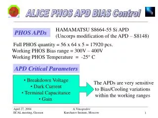
HAMAMATSU S8664-55 Si APD (Uncorps modification of the APD – S8148). PHOS APDs. Full PHOS quantity = 56 x 64 x 5 = 17920 pcs. Working PHOS Bias range = 300V – 400V Working PHOS Temperature = -25 ° C. APD Critical Parameters. Breakdown Voltage Dark Current Terminal Capacitance

PHOS APDs
E N D
Presentation Transcript
HAMAMATSU S8664-55 Si APD (Uncorps modification of the APD – S8148) PHOS APDs Full PHOS quantity = 56 x 64 x 5 = 17920 pcs. Working PHOS Bias range = 300V – 400V Working PHOS Temperature = -25° C APD Critical Parameters • Breakdown Voltage • Dark Current • Terminal Capacitance • Gain The APDs are very sensitive to Bias/Cooling variations within the working ranges
Why PHOS has need for individual APD BIAS Control ? PHOS takes part in ALICE Trigger by generation of partial analog energy sums. • So we must control the effective PHOS channel gain factors • to compensate the following scatterings: • Wide scattering of the APDs gain factors ; • Extreme sensitivity of the APDs gain to bias • for PHOS working temperature condition (-25C); • Gain scattering of the Preamps; • Light yield scattering of the PWO Crystals; • Scattering of the APD-Crystal gluing transparency. Individual APD BIAS Control has the benefit to refuse of APD’s selecting, grouping and pretest costs.
APD BIAS LV-HV regulation range HV (V) 400 Work HV range 300 250 Support voltage level 200 100 0 2.5 0 5 LV (V) 0 127 255 DAC code
General structure of Beam Test-2003 APD BIAS Control PHOS Cold zone 400V SPI Interface 8 DACs 8 Micro controller 8 T-card LV-HV 8 8 DACs 8 T-card LV-HV 32 APDs RS-232 Interface 8 DACs 8 8 T-card PC LV-HV 8 DACs 8 8 T-card LV-HV FEE SU To other SUs (512 channels)
Principle of Serial Peripheral Interface (SPI) SPI is a synchronous serial data protocol for a high bandwidth (1 megabaud) network connection amongst CPUs and other devices supporting the SPI.
Principle of DACs Daisy-Chaining 8DACs 8DACs 8DACs
LV-HV Regulator (I.Sibiriak) Minimum components schematic LV from DAC Output (0-5V) U ref 400V KPC452 AD8544 HV to APD (~250-400V)
Test Beam 2003 Kurchatov FEE view 8-Channels APD BIAS Regulator zone
Long-Term and Temperature Stabilities Test Results HV Long-Term Instability within 3 days < 0.1% HV Temperature Instability for 18 C° – 32 C° range < 0.1%
256 Channels PHOS GAINs Distribution (pre-selected APDs) Without APD BIAS Control
9 PHOS Central Channels (Wide Electron Beam) With APD BIAS Control • 8-bit DACs • (MAX5258) • 4% peak selection • accuracy
Evolution of APD BIAS Control after Test Beam 2003 1) More gain accuracy - from 4% (8-bit DACMAX5258) to 1% (10-bit DAC MAX5308); 2) Instead of Microcontroller use Readout Controller Unit (RCU) resources and Board Controller (BC) for DAC control (from ALICE TPC FEC project); 3) Separate control by 32 APD channels (one FEE); 4) SPI simulation on BC FPGA.
I2C SPI PHOS Cold zone 400V RCU Board Controller (FPGA) 8 DACs 8 I2C-SPI 8 T-card LV-HV 8 8 DACs 8 T-card LV-HV 32 APDs 8 DACs 8 8 T-card LV-HV ALTRO 8 DACs 8 8 T-card LV-HV FEE SU