Download
1 / 21
220 likes | 447 Views
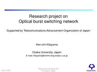
Osaka Univ. Research project on Optical burst switching network -Supported by Telecomunications Advancement Organization of Japan-. Ken-ichi Kitayama Osaka University, Japan E-mail: kitayama@comm.eng.osaka - u.ac.jp. Outline. Osaka Univ. Sponsored by

E N D
Osaka Univ. Research project onOptical burst switching network-Supported by Telecomunications Advancement Organization of Japan- Ken-ichi Kitayama Osaka University, Japan E-mail: kitayama@comm.eng.osaka-u.ac.jp Globecom’03 Workshop W-2 K. Kitayama, Japan
Outline Osaka Univ. • Sponsored by • Telecomunications Advancement Organization of Japan (TAO) • Participants • Coordinator : NTT Communications • NTT Network Innovations Laboratories • Fujitsu Laboratories • University of Tokyo • Osaka University • Period: 2001-2005 • Total budget: $15 million/5 years ($10 million in 2001-2003) Globecom’03 Workshop W-2 K. Kitayama, Japan
Current research projects on photonic networkssupported by the Japanese government PHASE II R&D? (2006-2010) Ultra-long & high-speed fiber optic transmissions (1996〜2005) Photonic node for broadband access (2000〜2005) Optical burst switching network (2001〜2005) Control plane for terabit networks (2001〜2005) Devices for photonic networks (2002〜2006) Globecom’03 Workshop W-2 K. Kitayama, Japan
Research subjects and their responsibilities- Aiming at high-efficiency photonic networking technology for bursty traffic - #1OBS network architecture and its control plane - NTT - #1OBS network architecture and its control plane - NTT - #2 Contention resolution and RWA - Univ. Tokyo - #3 Optical control packet - Osaka Univ. l0 Control l1 Data burst l2 Source node Destination node #4 Optical switch fabric - Fujitsu - Globecom’03 Workshop W-2 K. Kitayama, Japan
Switching time design target & application area - PHASE I: Photonic MPLS extension - LAN Metro Nation wide/Global Transmission Distance (L) 10km 100km 1000km 10,000 km Round trip delay 100ms 10ms 1ms 100ms 1TB (800s) 1000s Photonic MPLS Router at Present Next Generation DVD 30 GB Data Volume Transmitted By 10-Gbit/s signal h = 0.99 Signal length,tb 1s 1GB (0.8s) DVD 5 GB h = 0.9 CD 650 MB h = 0.5 1ms 1MB (0.8ms) 200msec at present Target Super High Definition Still Image 12 MB 100μs 1s 10s 1ms 100ms 10ms Switching Time tsw <=tsetup +tdown Network Throughput h <= tb / (tb + tsw ) Switching Timetsw (h= 1, L=0 km) Globecom’03 Workshop W-2 K. Kitayama, Japan
Switching time design target & application area - PHASE II: One-way protocol - LAN Metro Nation wide/Global . Transmission Distance (L) 10km 100km 1000km 10,000 km Round trip delay 100ms 10ms 1ms 100ms 1TB (800s) 1000s Photonic MPLS Router at Present Next Generation DVD 30 GB Data Volume Transmitted By 10-Gbit/s signal h = 0.99 Signal length,tb 1s 1GB (0.8s) DVD 5 GB h = 0.9 CD 650 MB h = 0.5 1ms 1MB (0.8ms) 200msec at present Target Super High Definition Still Image 12 MB 100μs 1s 10s 1ms 100ms 10ms Switching Timetsw (h= 1, L=0 km) Globecom’03 Workshop W-2 K. Kitayama, Japan
Demonstration of optical burst data switching- Photonic MPLS extension - 10 msec # 1 # i # 3 Bd2 Bd1 Monitor OLSP #1 OLSP #2 OLSP #1 (Obd1) OLSP #2 (Obd2) 160 msec Photonic MPLS Router developed by NTT Network Innovation Labs Optical burst data is transmitted by SDH STM-64 (@10Gb/s) framed signal. Condition; h= 1, L=0 km Globecom’03 Workshop W-2 K. Kitayama, Japan
Research subjects and their responsibilities- Aiming at high-efficiency photonic networking technology for bursty traffic - #1OBS network architecture and its control plane - NTT - #2 Contention resolution and RWA - Univ. Tokyo - #3 Optical control packet - Osaka Univ. l0 Control l1 Data burst l2 Source node Destination node #4 Optical switch fabric - Fujitsu - Globecom’03 Workshop W-2 K. Kitayama, Japan
3D-MEMS mirror structure 100 Parallel-Plate 10 Switching Time (ms) 1/10 10 mm 1 Comb-Driven 0.1 1 10 100 1000 Driving Voltage (V) Comb-driven MEMS Mirror Large Electro-Static Torque Low drive voltage, > 5-degree High-speed Switching Easy Controllability 80x80 Channels Globecom’03 Workshop W-2 K. Kitayama, Japan
Novel folded optical switch Targeting; 256x256 Ch. 2,000x2,000 Ch. Input/Output Fiber Array Roof-type Retro-reflector Input/Output Micro-lens Array 80x80 Channels Input/Output MEMS Mirror Array Size: 87 x 77 x 53 mm Folded Configuration with Roof-type Retro-reflector by a factor of 1/2 of Flat-reflector (Lucent) Insertion Loss: 3 dB Crosstalk: < -40 dB Globecom’03 Workshop W-2 K. Kitayama, Japan
Optical switch module 1ms Optical Switch Optical Switch B A B In #1 Out #1 In #1 Out #1 In #2 Out #2 In #2 Out #2 In #1 Burst B Burst A 80x80 Channels In #2 Feed-forward Control Switching Size: 150(W) x 400(H) x 300(D) mm Out #1 H: 1ms/div Burst B Burst A Supply Voltage: 200 V Power Consumption: 22 W Globecom’03 Workshop W-2 K. Kitayama, Japan
Research subjects and their responsibilities- Aiming at high-efficiency photonic networking technology for bursty traffic - #1OBS network architecture and its control plane - NTT - #2 Contention resolution and RWA - Univ. Tokyo - #3 Optical control packet - Osaka Univ. l0 Control l1 Data burst l2 Source node Destination node #4 Optical switch fabric - Fujitsu - Globecom’03 Workshop W-2 K. Kitayama, Japan
Deflection routing F G H I J With Deflection A B C D E Without Deflection • Deflect blocked bursts to idle fiber links • Save bandwidth • A dropped burst wastes the bandwidth on the partially established path • Save time • The delay becomes very large when retransmitting a blocked burst in long-distance links Globecom’03 Workshop W-2 K. Kitayama, Japan Univ.Tokyo
Priority-based wavelength assignment • Each sender keeps a wavelength priority database for every destination node. By learning from the statistical data of prior transmission results, each node ranks wavelengths for giving prioritized wavelength assignment. As learning progresses, wavelength spatial reuse becomes possible Globecom’03 Workshop W-2 K. Kitayama, Japan
Research subjects and their responsibilities- Aiming at high-efficiency photonic networking technology for bursty traffic - #1OBS network architecture and its control plane - NTT - #2 Contention resolution and RWA - Univ. Tokyo - #3 Optical control packet - Osaka Univ. l0 Control l1 Data burst l2 Source node Destination node #4 Optical switch fabric - Fujitsu - Globecom’03 Workshop W-2 K. Kitayama, Japan
Tell-and-go protocol using OC-label (OC-TAG) Offset time Offset time Distance Source Destination • OC-label processing for control packet • OC-labeled control packet neglects the processing time Processing delay ~ 0 Time Data transmission Burst data Release signal for unlimited burst duration Globecom’03 Workshop W-2 K. Kitayama, Japan
Blocking probability: JET vs. OC-TAG Osaka Univ. • Blocking probability: number of blocked requests / number of requests • Processing delay at node: 1.0ms (JET case) • Number of wavelengths: 32 or 64 • No retransmission if data loss occurs Mean blocking probability Arrival rate Globecom’03 Workshop W-2 K. Kitayama, Japan
OC-label processing for control packet OC-labeled control packet on out-of-band wavelength l0 OC-lable for l OC-label for LSP OC Ultrafast setup of optical path Osaka Univ. Electrical processing OC-label processor O/E E/O OC’ Offset time Optical switch Burst data Globecom’03 Workshop W-2 K. Kitayama, Japan
Experimental OC-labeled control packet processings Auto-correlation Cross-correlation Osaka Univ. 0p p p p 0 Labels R1 Labels R1 l1 l1 8-chip OC-label 20mV/div 100ps/div Label swapping from R1 to R2 Optical mask l1 l2 l1 l2 Label R1 recognition Encoder4 SA PPG 20mV/div 20mV/div Gate signal generator LN-IM Decoder1 100ps/div 1×2 Switch Encoder3 l2 l1 l2 R2 R2 l1 Add the available wavelength l2 20mV/div 20mV/div Globecom’03 Workshop W-2 K. Kitayama, Japan
Summary Osaka Univ. • National R&D project, particularly focus on OBS • Comprehensive program from optical switch, transport plane, control plane, and management plane • Field trials in the network testbed planned; • PHASE I in 2003-2004: Photonic MPLS extention • PHASE II in 2005: Novel RWA & OC-label processing Globecom’03 Workshop W-2 K. Kitayama, Japan
Thank you! Globecom’03 Workshop W-2 K. Kitayama, Japan