Download
1 / 39
390 likes | 694 Views
Chap 5. Registers and Counters. 5.1 Definition of Register and Counter. a clocked sequential circuit consist of a group of flip-flops & combinational gates connected to form a feedback path Registers & Counters -- sequential circuits with F-F Register include a set of F-Fs

E N D
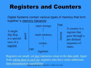
5.1 Definition of Register and Counter • a clocked sequential circuit • consist of a group of flip-flops & combinational gates connected to form a feedback path • Registers & Counters -- sequential circuits with F-F • Register • include a set of F-Fs • each F-F is capable of storing one bit of information = n-bit registers includes n F-Fs • (broadest def) consists of a set of F-Fs, together with gates that implement their transition • (narrower def) register: a set of F-Fs (hold data) gates: perform data-processing tasks (determine the new and transformed data to be transferred into the F-Fs)
5.1 Definition of Registers and Counters • Counter • a register that goes through a predetermined sequence of states upon the application of clock pulses • gates are connected to produce the prescribed sequence of states • a special type of register, but common to differentiate from registers • Registers and Counters • sequential functional blocks, used in the design of digital systems • Registers: useful for storing and manipulating information • Counters: generate timing signals to sequence and control operations
5.2 Registers • (simplest register) consists of only F-Fs w/o any external gates
5.2 Registers • 4-bit Register • 4 D-type F-Fs • common Clock input triggers all F-Fs on the rising edge of each pulse • binary data at the 4 inputs are transferred into 4-bit register • 4 Q outputs can be sampled to obtain the binary information • clear' input (R') • when 0, reset all F-Fs asynchronously • login-1 during normal operations • loading : transfer of new info into a register • parallel : all the bits of the register are loaded simultaneously
5.2 Registers • Register with Parallel Load • a load control input: • a separate control signal to decide which specific clock pulse will have an effect on a particular register • can be done with a load control input ANDed with the clock C input = Load' + Clock • Inserting an AND gate in the path of clock pulses => logic is performed with clock pulses => produce different propagation delays between Clock and the inputs of F-Fs (clock skew problem)
5.2 Registers • 4-bit Register • 4-bit register with a control input • Clock inputs receive clock pulses always • Load input determines the action to be taken w/ each clock pulse • if Load =1, data are transferred into the register w/ the next positive transition of a clock pulse • if Load =0, data inputs are blocked & the D inputs of F-Fs are connected to their outputs (feedback connection is necessary)
5.3 Shift Registers • a register capable of shifting its stored bits in one or both directions • consists of a chain of F-Fs in cascade w/ output of one F-F connected to the input of the next F-F • receive common clock pulse
5.3 Shift Registers • 4-bit Shift Registers • the output of a F-F is connected to the D input of F-F at its right • Clock is common • serial input SI is the input to the leftmost F-F • serial output SO is taken from the output of the rightmost F-F • Serial Transfer • Operate in a serial mode when info is transferred and manipulated one bit at a time • by shifting the bits out of one register and into a second (cf) parallel transfer
5.3 Shift Registers • Serial Transfer Circuit • serial output of A is connected to the serial input of B • serial control input Shift determines when and how many times the registers are shifted • in the figure, each shift register has 4 stages
5.3 Shift Registers • the control unit must be designed to enable the shift registers • serial mode: registers have a single serial input & output info is transferred one bit at a time • parallel mode: info is available from all bits of a register & all bits can be transferred simultaneously
5.3 Shift Registers • Serial Addition • Operations in digital computers are usually done in parallel since it is a faster !! • Serial operations are slower, but requires less hardware • Serial adder (cf) parallel adder (Section3.8, Figure3.28 p128) • two binary numbers are stored in 2 shift registers, • bits are added one pair at a time through a single FA
5.3 Shift Registers • A carry out of FA is transferred into a D F-F (used as the input carry for the next addition) • Sum bit on the S output of FA is transferred into a third shift register, but transfer it into register A (contents of A are shifted out) (serial input of B can receive a new binary number)
5.3 Shift Registers • Initial assignment • register A holds the augend; • register B holds the addend; • carry F-F is reset to 0 • Operation • the shift control enables the clock for registers and the F-F • for each pulse, • a new sum bit is transferred to A, • a carry is transferred to the F-F, & • both registers are shifted once to the right • (other possibility) • initially clear register A to 0 & add the first number from B • then number in B is shifted to A through the FA, and the second number is transferred serially into B • then the second number is added to the contents of A
5.3 Shift Registers • Comparison (space-time trade-off) • parallel adder: • use a register with parallel load • No of full adder circuits is equal to No of bits in binary number • a combinational circuit (excluding registers) • serial adder: • use shift registers • an example of iterative logic array • requires only one full adder and a carry F-F • a sequential circuit since it include carry F-F
5.3 Shift Registers • Shift Register with Parallel Load • data entered in parallel can be taken out in serial fashion by shifting out the data in the register • used for converting incoming parallel data to outgoing serial transfer and vice versa
5.3 Shift Registers • 2 control inputs: one for shift & one for load • each stage consists of a D F-F, an OR gate and 3 AND gates • first AND: enables the shift operation • second AND: enables the input data • third AND: restores the contents of the register (when no operation is required) • If shift=0 & load=0, 3rd AND is enabled, output of each F-F is applied to its D input • If shift=0 & load=1, 2nd AND is enabled, input data is applied to each D input • If shift=1 & load=0, 1st AND is enabled, transfer data to the next F-F • used to interface digital system • transmitter: parallel-to-serial conversion • receiver: serial-to-parallel conversion
5.3 Shift Registers • Bidirectional Shift Register shift in both directions (cf) unidirectional shift register shift in one direction only • possible to modify circuit of Fig 5.6 by adding a 4th AND gate in each stage 4 AND gates + 1 OR gate constitute a multiplexer
5.3 Shift Registers • Each stage consists of a D flip-flop & a 4-to-1-line multiplexer
5.4 Ripple Counters • Counter • a register that goes through a prescribed sequence of states upon the application of input pulses • input pulse: clock pulse, or from some external source • follow the binary number sequence or other sequence of states • an n-bit binary counter • consists of n F-Fs • can count from 0 up to 2n-1 • Ripple counters vs Synchronous counters • ripple counters • F-F output transition serves as a source for triggering other F-F • all F-Fs are triggered not by common clock pulses, but by the transition that occurs in other F-F outputs • synchronous counters • all F-Fs receive the common clock pulse • the change of state is determined from the present state
5.4 Ripple Counters • constructed with F-Fs capable of complementing their contents, such as JK • output of each F-F is connected to the C input of the next F-F • the F-F holding LSB receives the incoming clock pulse • J & K inputs of all F-F are connected to 1 (permanent logic-1) • negative-edge triggering (small circle on C indicates it)
5.4 Ripple Counters • LSB A0 is complemented with each count pulse input • Every time that A0 goes from 1 to 0, it complement A1
5.4 Ripple Counters • Binary Down-Counter • decremented by one with every input count pulse (cf) up-counter -- incremented by one • From Fig 5.8, but take the outputs from the complement outputs of the F-Fs 1) complement output of each F-F to the C input of the next 2) uses positive-edge-triggered F-Fs • Advantages & Disadvantages • simple hardware • asynchronous with added logic unreliable & delay-dependent • incompatible with modern system design
5.5 Synchronous Binary Counters • clock pulses are applied to the inputs of all F-F (different from ripple counters !!) • common clock pulses are applied to the inputs of all of the F-Fs • Design of Binary Counter • design procedure for a synchronous counter • same as with any other synchronous sequential circuit • operate without an external input except for the clock pulses • output of the counter is taken from outputs of the F-Fs without any additional outputs from gates • state table of a counter consists of columns for the present state & next state only
5.5 Synchronous Binary Counters • State table
5.5 Synchronous Binary Counters • Binary counters are most efficiently constructed with complementing T or JK F-Fs (also with D F-Fs) • Obtain the F-F inputs for each J & K (use excitation cond) • Simplify the input equations by maps
5.5 Synchronous Binary Counters • JQ0 & KQ0 equal to 1 (maps contain only 1's and X's) • equations for J & K are the same for each F-F • T F-F could be used instead of JK • input equations w/ count enable input EN can be expressed as JQ0 = KQ0 = EN; JQ1 = KQ1 = Q0 EN; JQ2 = KQ2 = Q0Q1 EN; JQ3 = KQ3 = Q0Q1Q2 EN; • F-F in the LSB is complemented with every clock pulse transition • a F-F in any other position is complemented w/ a clock trans if all least significant bits are equal to 1 => in an n-bit binary counter, Qi at any stage of i is JQi = KQi = Q0Q1 ...... Qi-1 EN;
5.5 Synchronous Binary Counters • Synchronous binary counters have a regular pattern • C inputs of all F-Fs receive the common clock pulses • the chain of AND gates generates the required logic for the J & K inputs • the carry output CO can be used to extend the counter to more stages • F-Fs trigger on the positive-edge transition of the clock • but the polarity if the clock is not essential here
5.5 Synchronous Binary Counters • Counter with D Flip-Flops • input equations can be expressed in sum of minterms as a function of the present state DQ0(Q3,Q2, Q1, Q0) = m(0,2,4,6,8,10,12,14); DQ1(Q3,Q2, Q1, Q0) = m(1,2,5,6,9,10,13,14); DQ2(Q3,Q2, Q1, Q0) = m(3,4,5,6,11,12,13,14); DQ3 (Q3,Q2, Q1, Q0) = m(7,8,9,10,11,12,13,14); • simplifying 4 equations with maps DQ0 = Q0 EN; DQ1 = Q1 (Q0 EN) DQ2 = Q2 (Q0 Q1 EN); DQ3 = Q3 (Q0 Q1 Q2 EN) • DQi = Qi (Q0 Q1 Q2 .... Qi-1 EN)
5.5 Synchronous Binary Counters • Serial and Parallel Counters • in Fig(a), a chain of 2-input AND gates is used • analogous to the carry logic in the ripple carry adder • a counter has serial gating, referred to as a serial counter • in Fig(b), • a counter has parallel gating, referred to as a parallel counter • from 1111 to 0000, only 1 gate delay occurs (instead of 4)
5.5 Synchronous Binary Counters • Up-Down Binary Counter • synchronous count-down binary counter goes through the binary states in reverse order from 1111 to 0000 and back to 1111 • the result is predictable • the bit in LSB is complemented with each count pulse • bit in any other position is complemented if all lower bits are equal to 0 • the next state after the present state of 0100 is 0011 • the logic diagram is similar to that of the binary up-counter • inputs to the AND gates must come from the complemented outputs of the F-Fs
5.5 Synchronous Binary Counters • 2 operations can be combined • use T F-Fs TQ0 = EN; TQ1 = Q0 S EN + Q0' S' EN; TQ2 = Q0 Q1 S EN + Q0' Q1' S' EN; TQ3 = Q0 Q1 Q2 S EN + Q0' Q1' Q2' S' EN; • the output carries for the next state are Cup = Q0 Q1 Q2 Q3 S EN Cdn = Q0' Q1' Q2' Q3' S' EN
5.5 Synchronous Binary Counters • Binary Counter with Parallel Load • logic diagram of a register with parallel load + counter
5.5 Synchronous Binary Counters • Synchronous BCD Counter • a binary counter with parallel load can be converted by connecting an external AND gate • It starts with all-zero output, and the counter input is active at all times • as long as the output of the AND gate is 0, each positive clock pulse transition increments the counter by one • when output reaches 1001, both Q0 & Q3 become 1 Load active 0000 is loaded into the counter
5.6 Other Synchronous Counters • Counters are designed to generate any desired number of sequence • A divide-by-N counter (modulo-N counter) is a counter that goes through a repeated sequence of N state • the sequence may follow the binary count, or may be any other arbitrary sequence • BCD Counter • obtained from a binary counter with parallel load • possible to design a BCD counter with individual F-Fs & gates • derive the state table and input conditions with T F-Fs
5.6 Other Synchronous Counters • simplified by means of maps TQ1 = 1; TQ2 = Q1Q8'; TQ4 = Q1Q2; TQ8 = Q1Q8 + Q1Q2Q4; Y = Q1Q8 • implemented with 4 T F-Fs, 5 AND gates, 1 OR gate
5.6 Other Synchronous Counters • Arbitrary Count Sequence • design a counter that has a repeated sequence of 6 states • 011 & 111: unused states • implement with JK F-Fs JAC = B; KA = B; JB = C; KB = 1; JC = B'; KC = 1;
5.6 Other Synchronous Counters • JAC = B; KA = B; JB = C; KB = 1; JC = B'; KC = 1; • 2 unused states • next count pulse transfers it to one of the valid states & continues to count correctly (self-correcting)