Download
1 / 37
760 likes | 2.1k Views
An Introduction to Band Theory, A Molecular Orbital Approach. Chemistry 754 Solid State Chemistry Dr. Patrick Woodward Lectures #17-18. References – Band Theory.

E N D
An Introduction to Band Theory, A Molecular Orbital Approach Chemistry 754 Solid State Chemistry Dr. Patrick Woodward Lectures #17-18
References – Band Theory The material for this lecture comes primarily from the work of Roald Hoffmann and those who came through his group (Mike Whangbo, Jeremy Burdett, Thomas Albright, Tim Hughbanks, etc.). His treatment (and many of the figures used in this lecture) are nicely summarized in a small book he wrote some years ago: “Solids and Surfaces: A chemists view of bonding in extended structures” Roald Hoffmann, VCH Publishers, (1988) See also “The Electronic Structure and Chemistry of Solids” P.A. Cox, Oxford University Press, Oxford (1987). “Chemical Bonding in Solids” Jeremy K. Burdett, Oxford University Press, Oxford (1995).
Relevance of Band Structure • What is the electronic band structure? • For an extended solid the band structure plays the same role that an MO diagram does for a molecule. • Why it is important to be able to comprehend the electronic band structure? • The band structure is the link between crystal structure, bonding and properties. In particular details of the band structure are closely linked to the following properties: • Electronic conductivity • Optical properties, including color • Electronically driven structural distortions • Mechanical and Magnetic Properties • Catalytic Activity
MO Diagram ReO66- Octahedron In the last lecture we discussed the MO diagram of an octahedron (shown to the left). How does this diagram change when we have an extended structure?
Band Structure ReO3 Band Structure (aka Spaghetti diagram): MO diagram with translational symmetry taken into account. Density of States (DOS) Integration of the band structure. Shows the # of available levels between E and E+dE as dE 0.
Constructing a DOS Diagram: TiO2 It’s possible to construct a reasonable approximation of the DOS diagram from the MO diagram of the building block. The energy levels of each block of bands or “BOB” comes from the MO diagram (based on electronegativity and bonding interactions) The area of each BOB is proportional to the number of MO’s at that approximate energy. The width of each BOB is derived from the overlap between building blocks
Constructing a DOS Diagram: TiO2 The DOS plots for TiO2(rutile), SrTiO3 (perovskite), CaTiO3 (cubic perovskite) and MgTiO3 (ilmenite) are all going to be qualitatively similar, because the electronic building block is the same in each case, the TiO6 octahedron. The electropositive cations: such as Sr2+, Ca2+ and Mg2+ only make minor contributions near the Fermi energy. The main difference will be the width of the bands (as the octahedra are connected differently in each structure). Ti eg Ti-O s* Ti t2g Ti-O p* Ef O 2p, Ti-O bonding O 2s
H2 Molecule Chain of 5 H atoms c0 c1 c2 c3 c4 E Antibonding 4 c1 c2 3 Nonbonding 2 1 Bonding 0 # of Nodes
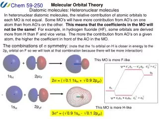
c0 c1 c2 c3 c4 k=p/a k=p/2a k=0 a Infinite 1D Chain of H atoms If there are N atoms in the chain there will be N energy levels and N electronic states ("MOs"). The wavefunction for each electronic state is: Yk = S eiknacn Where: • a is the lattice constant (spacing between H atoms), • n identifies the individual atoms within the chain, • cnrepresents the atomic orbitals • k is a quantum # that identifies the wavefunction and tells us the phase of the orbitals.
c0 c1 c2 c3 c4 k=p/a k=p/2a k=0 a Infinite 1D Chain of H atoms k = p/a Yp/a = c0+(exp{ip})c1 +(exp{i2p})c2 +(exp{i3p})c3+(exp{i4p})c4+… Yp/2a = c0 - c1 + c2 - c3 + c4 +… k = p/2a Yp/2a = c0+(exp{ip/2})c1 +(exp{ip})c2 +(exp{i3p/2})c3+(exp{i2p})c4+… Yp/2a = c0 + 0 - c2 + 0 + c4 +… k = 0 Y0 = c0+c1 +c2 +c3 +c4 +… k=0 orbital phase does not change when we translate by a k=p/a orbital phase reverses when we translate by a
Band Structure Linear H Chain E(k) EF 0 k p/a • The Fermi energy separates the filled states (E < EF at T = 0 K) from the empty states (E > EF at T = 0 K). Here it splits the band (each band can hold 2 electrons) • A 1D chain of H atoms is predicted to be metallic because the Fermi level cuts a band (there is no gap so it takes only an infinitesimal energy to excite an electron into an empty state). • The band runs "uphill" (from 0 top/a) because the in phase (at k=0) combination of orbitals is bonding and the out of phase (at k=p/a) is antibonding.
Effect of Orbital Overlap • If we reduce the lattice parameter a it has the following effects: • The spatial overlap of the orbitals increases • The band becomes more bonding at k=0 • The band becomes more antibonding k=p/a. • The increased antibonding is larger than the increased bonding. • The bandwidth increases. • The electron mobility increases. • Wide bands Good orbital overlap High carrier mobility
EF EF EF E(k) EF p/a p/a p/a p/a 0 0 0 0 k k k k Band Structure: Linear Chain of F F F F F F F F F F F (a) (b) (c) (d) Which of the following is the correct band structure for a linear chain of F atoms?
Band Structure: Linear Chain of F Antibonding 2pzs* Doubly degenerate EF Antibonding 2px/2pyp* Doubly degenerate Antibonding 2s s* Bonding 2px/2pyp Bonding 2pz s Bonding 2s s 0 k p/a
Band Structure: Linear Chain of F A more accurate treatment of the band structure would show an avoided crossing between the 2pzs and 2s s * interactions at k=p/a. There would be mixing between these two bands (creating sp-hybrid like states) similar to the 2s/2p s & s* interactions seen in the MO diagram of N2. Antibonding 2pzs* EF Doubly degenerate Bonding 2px/2pyp Bonding 2s s 0 k p/a
Lessons from Linear F Chain • There are now 4 orbitals in the unit cell (a single F atom with 1 2s + 3 2p orbitals) giving rise to 4 bands in the band structure. • The fact that the wavefunction corresponding to a p-orbital changes sign at the nucleus causes the 2p s band to run downhill (opposite of the 2s s band). • The reduced spatial overlap of the p interaction causes the p bands to be narrower than the s bands. • The 2p orbitals start out at a higher energy than the 2s orbitals (from atomic quantum theory)
More than 1 atom in the Unit CellThe Pierls Distortion What happens when there is more than one atom in the unit cell? To illustrate the consequences consider a distortion of the 1D chain of H atoms which causes the atoms to dimerize. The consequences will be as follows: • There are now 2 orbitals in each unit cell, so there will be 2 bands in the band structure. • Let’s construct 1 band to be bonding within the unit cell (HOMO - valence band), and the other to be antibonding within the unit cell (LUMO - conduction band). • Translational symmetry and the value of k will take care of the rest.
c0 c1 c2 c3 c4 c5 k=p/a k=p/2a k=0 Pierls Distortion (H2 Chain) Conduction Band (LUMO s*) Intra Inter c0 c1 c2 c3 c4 c5 s*s k=p/a s* s Band runs downhill s* non k=p/2a s*s * k=0 Valence Band (HOMO s) Intra Inter ss* s s * Band runs uphill s non ss
E(k) EF p/a 0 k Band Structure H2
Lessons – Pierls Distortion (H2) • There are two electrons per unit cell so that the valence band is full and the conduction band empty. Thus EF occupies a position midway between the two bands and the system is now a semiconductor/insulator. • The minimum energy gap between bands occurs at k = p/a. Since the maximum in the VB and the minimum in the CB occur at the same value of k, the compound is said to be a direct gap semiconductor. • Compared with the band structure of a linear chain of hydrogen atoms the bands in this system will be narrower. This is a consequence of the reduced overlap between molecules. • The net effect of this distortion is to lower the energy of the filled states (which originate from bonding MO’s) while raising the energy of empty states (antibonding MO’s). In 1D such a distortion will always be stable when you have a half filled band (as we did in the H band structure). Physicists call this a Peierls distortion, it is the solid state equivalent of a 1st order Jahn-Teller distortion.
PtH4 a Molecular Chain Compound Now let’s consider a compound that contains different types of atoms within the unit cell. The compound A2PtX4 (where A is a +1 cation, such as K+, and X –1 anion, such as Cl-, CN- or H-) forms linear chains and is a good example to consider. Let’s construct the band structure of PtH42- (the K+ are very electropositive and serve primarily as donors of electrons, we will ignore them except when it comes to counting electrons). The process consists of 3 steps. Step 1: Consider the MO Diagram of the Building unit (here a PtH4 Square Planar Unit). This gives an idea of the band energy levels. Step 2: Consider the orbital overlap between units (molecules in this case). This tells us if the bands run uphill or downhill. Step 3: Consider the degree of orbital overlap (spatial and energetic) between units. This gives the band widths.
H H H H H H H H Pt Pt Pt Pt H H H H H H H H Linear PtH4 Chain Step 1: Consider the MO Diagram of the Building unit (here a PtH4 Square Planar Unit). This gives an idea of the band energy levels.
Linear PtH4 Chain Step 2: Consider the orbital overlap between units (molecules in this case). This tells us if the bands run uphill or downhill.
Linear PtH4 Chain Calculated Band Structure Step 3: Consider the degree of orbital overlap (spatial and energetic) between units. This gives the band widths.
Geometry and Properties Consider the salt K2PtH4 (or K2PtCl4) and predict what would be it’s optimal geometry and properties. Which configuration would be more stable a staggered (PtH4 units rotated by 45º to each other) or an eclipsed geometry (PtH4 units related by a mirror plane)? Would you expect this material to be a semiconductor or a metal? How would the Pt-Pt distance react if the material were oxidized?
K2Pt(CN)4 Pt2+ (d8) - dz2 band is completely filled Pt-Pt distance = 3.3 A Eclipsed geometry (the Pt-Pt distance is too long for Pt-Pt p interactions to matter). Semiconductor (Fermi level falls between dz2 band and the dx2-y2 band) K2Pt(CN)4Cl0.3 Pt2.3+ (mixed d7/d8) - dz2 band is partially filled Pt-Pt distance = 2.7 A (electrons have been removed from Pt-Pt antibonding states Staggered geometry (minimize dxz-dxz and dyz-dyz interactions) Conductor (Fermi Level cuts dz2 band) K2Pt(CN)4Clx
Two dimensions G= (kx=0, ky=0, kz=0) X = (p/a, 0, 0) M = (p/a, p/a, 0) Y = (0, p/a, 0) R = (p/a, p/a, p/a) Z = (0, 0, p/a)
z y x Band Structure of Ba2SnO4 To give a real example of a band structure which is predominantly two dimensional consider the Ruddlesden-Popper compound Ba2SnO4. This compound contains sheets of corner sharing octahedra. Let’s derive the band structure for one of these sheets.
Constructing the Band Structure Step 1: Consider the MO Diagram of the building unit. In this case the building unit is a SnO6 octahedron. The 4d orbitals of Sn are essentially core orbitals and can be neglected. The 2s orbitals of oxygen play a role, but for the sake of simplicity they will be ignored. Step 2: Consider the orbital overlap between units. In this case the Sn 5px-O 2px, the Sn 5py-O 2py, and the Sn 5s-O 2px/O 2py interactions need to be considered. The Sn 5pz-O 2pz interactions are essentially isolated on individual building units and will give rise to flat bands. Step 3: Consider the degree of orbital overlap. Both the Sn 5s-O 2p and Sn 5p-O 2p interactions have a favorable spatial overlap. The Sn 5s-O 2p interaction has a better energetic overlap though.
2t1u Sn 5p 2a1g Sn 5s * eg eg O 2p t1u 1t1u a1g 1a1g SnO6 MO Diagram *In total there are 36-4 = 14 non-bonding O 2p orbitals (neglecting p-bonding and Sn 4d overlap). Only two are shown here.
Sn 5s-O 2p Valence Band Majority O 2p character Sn 5s-O 2p Conduction Band Majority Sn 5s character y y x x G G O 2p Nonbonding Sn 5s Nonbonding X X Sn 5s-O 2p Bonding Sn 5s-O 2p Antibonding M M
Sn 5px-O 2px Valence Band Majority O 2p character Sn 5px-O 2px Conduction Band Majority Sn 5p character y y x x Sn 5p-O 2p Bonding Sn 5p-O 2p Antibonding G G X X O 2p Nonbonding Sn 5p Nonbonding M M
Sn 5py-O 2py Valence Band Majority O 2p character Sn 5py-O 2py Conduction Band Majority Sn 5p character y y x x Sn 5p-O 2p Bonding Sn 5p-O 2p Antibonding G G X X Sn 5p Nonbonding O 2p Nonbonding M M
Ba2SnO4: Band Structure Sn 5pZ-O 2pZs* Sn 5py-O 2pys* Sn 5px-O 2pxs* Sn 5s-O 2p s* EF Band Gap O 2p nonbonding Sn 5py-O 2pys Sn 5px-O 2pxs Sn 5pZ-O 2pZs Sn 5s-O 2p s G X M G
3D: The Band Structure ReO3 We can now go full circle and return to the ReO3 spaghetti diagram that started our discussion. The band structure of this compound is similar in many ways to the Ba2SnO4 band structure. The main differences are: • Because of the 3-dimensionality all of the Re based bands will be disperse (only O 2p non-bonding states will give rise to flat bands). • The most important interactions are the Re 5d-orbitals, t2g (p/p*) & eg (s/s*), rather than the Sn 5s & 5p. • The Fermi level cuts the p* bands creating a metallic conductor rather than a semiconductor.
ReO3 Bandstructure Overlap at the M-point kx=ky=p/a, kz=0 Re Re O O O Re Re O Re Re O O O Re Re O O 2p nonbonding p* p* Overlap at the G-point kx=ky=kz=0 p* The points circled in blue are the bonding counterparts to the antibonding interactions shown to the right. p G point non-bonding W(t2g/p*) ~ 5 eV W(eg /s*) ~ 7 eV The eg/s* band is wider than t2g/p* due to larger orbital overlap (spatial).
Summary Band Structures • What is being plotted?Energy vs. k, where k is the wavevector that gives the phase of the AO’s as well as the wavelength of the electron wavefunction (crystal momentum). • How many lines are there in a band structure diagram?As many as there are orbitals in the unit cell. • How is the center of gravity energy level of each band determined?Usually follows from the MO diagram. • How do we determine whether a band runs uphill or downhill?By comparing the orbital overlap at k=0 and k=p/a. • How do we distinguish metals from semiconductors and insulators?The Fermi level cuts a band in a metal, whereas there is a gap between the filled and empty states in a semiconductor. • Why are some bands flat and others steep?This depends on the degree of orbital overlap between building units. Wide bands Large intermolecular overlap delocalized e- Narrow bands Weak intermolecular overlap localized e-