Download
1 / 1
10 likes | 113 Views
Study of the Sn-Zn-X alloys for solder applications in the electronic industry. WORKING TEAM IN GROUP PROJECT GP5 : Portugal: Finland: Bulgaria: France:. Univ. of Minho, Dep. Mechanical Eng. Physical Dep. Univ. of Porto Materials Eng. Dep. Peixinhos, Lda.

E N D
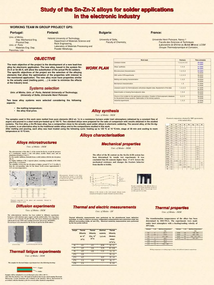
Study of the Sn-Zn-X alloys for solder applications in the electronic industry WORKING TEAM IN GROUP PROJECT GP5: Portugal: Finland: Bulgaria: France: Univ. of Minho, Dep. Mechanical Eng. Physical Dep. Univ. of Porto Materials Eng. Dep. Peixinhos, Lda Helsinki University of Technology, Department of Materials Science and Rock Engineering Laboratory of Materials Processing and Powder Metallurgy University of Sofia, Faculty of Chemistry Universite Henri Poincare, Nancy 1 Faculte des Sciences et Techniques Laboratoire de Chimie du Solide Mineral, LCSM Groupe Thermodynamique et Corrosion OBJECTIVE The main objective of the project is the development of a new lead-free alloy for electronic application. The new alloy, based in the system Sn-Zn-X or Sn-Bi-X, will allow the substitution of the actual Pb-Sn solders. The specific objectives of the project are the selection of the alloying elements that allow the optimization of the properties with interest to the mentioned application. The new alloy must have properties similar to the actually used (melting point, …) in order to minimize the effects at the industry level. WORK PLAN • Systems selection • Univ. of Minho, Univ. of Porto, Helsinki University of Technology, University of Sofia, Universite Henri Poincare • Two base alloy systems were selected considering the following aspects: • the melting temperature; • the alloy final price. Alloy synthesis Univ. of Minho - DEM Chemical composition, obtained by XRF spectrometry, of the melted alloys The samples used in this work were melted from pure elements (99.9 wt. %) in a resistance furnace under inert atmosphere (obtained by a constant flow of argon) and poured in a steel mold pre-heated up to 100 ºC. Two standard alloys were prepared for the sake of comparison with results obtained in the studied systems. The first alloy, a Sn-Pb base alloy, has a composition close to the actually used solder alloys in electronic soldering. The second alloy, of the Sn-Ag-Cu system, is an alternative alloy to the traditional solder alloys and to the compositions studied in this work. After melting and pouring, each alloy was heat treated using the following cycle: heating up to 120 ºC at 10 ºC/min, stage of 30 min and cooling to room temperature at 10 ºC/min. Alloys characterisation Alloys microstructures Univ. of Minho - DEM Mechanical properties Univ. of Minho - DEM The microstructure of the alloy 1, of the system Sn-Zn-Al, reveals the presence of 3 constituents: matrix, a zinc rich phase, needles (black zone) and an aluminum rich phase (“stars”). For the smaller additions, bismuth forms a solid solution with the tin rich phase (fig. b). For higher additions of Bi, a separate phase, consisting essentially of Bi (white phase in fig. c), is formed. The solubility of Bi in the tin rich phase is higher, around 3.7 wt % in alloy 6, than the corresponding value for the binary Sn-Bi system (approximately 1 wt% at room temperature). The effect of the Bi content on the Sn-Zn-Al-Bi system has been determined by tensile test experiments. It was concluded that Bi contents higher than ~5 wt% lowers the mechanical resistance and changes the fracture behavior from ductile to brittle. Microstructures obtained in the alloys, with different Bi contents: a) with 0%Bi; b) with 0.9 wt% Bi; c)with 6.9 wt% Bi (magnifications of 500X). Fracture morphology of the different alloys a) and detail of the ductile and brittle fracture b) for, respectively, alloys 1 (0 wt.% Bi), 4 (3.3 wt.%Bi) and 6 (6.9 wt.%Bi). Influence of Bi contents on the yield strength, ultimate tensile strength and elongation at rupture obtained inproduced alloys. Chemical composition of the phases and constituents, obtained by SEM/EDS, in alloys 1 and 6. Diffusion experiments Univ. of Minho - DEM Thermal and electric measurements Univ. of Minho - DF Thermal properties Univ. of Minho - DEM The solder/substrate interface has been studied by diffusion experiments, between a solid substrate (pure copper) and the melted solder. Two stage times, at 250 ºC, were selected: 30 and 120 min. The layers obtained were studied by optical microscopy (OM) and scanning electronic microscopy (SEM/EDS). Several layers were detected for the Sn-Zn-Al and Sn-Zn-Al-Bi solders. Thermal diffusivity measurements were performed by the photothermal beam deflection technique. In order to improve accuracy, independent measurements were performed under two different surrounding media, air and CCl4. Electrical resistivity measurements were performed by the four probe method. The transformation temperatures of the alloys has been determined by DSC/TGA. The experiments were made under inert atmosphere with a heating/cooling velocity of 10ºC/min. Melting temperature (or melting range) of alloys with different chemical compositions. Thermall fatigue experiments Univ. of Minho - DEM The samples for thermal fatigue experiments have the following drawing: Copper Solder Samples will be submitted to several thermal cycles (-40 to 120 ºC). After that the interface zone will analysed byptical microscopy and Scanning Electronic Microscopy. Cracks formation and evolution at the interface will be characterised in accordance with the thermal cycles for several solder chemical compositions.