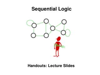
Understanding Sequential and Combinatorial Components in Digital Circuits
This comprehensive guide explores the intricacies of sequential and combinatorial components in digital circuits, discussing flip-flops, clocking, memory elements, and more. Learn about asynchronous and synchronous circuits, types of flip-flops, and how to implement different functionalities using various components. Dive into the world of sequential logic and understand the fundamental concepts through practical examples.


Understanding Sequential and Combinatorial Components in Digital Circuits
E N D
Presentation Transcript
Sequential Logic • Combinatorial components: the output values are computed only from their present input values. • Sequential components: their output values are computed using both the present and past input values. • Sequential circuits can contain only a finite number of states finite state machines • Synchronous and Asynchronous
Sequential Circuits • Contains Memory Elements • Asynchronous sequential circuits change their state and output values when input changes • Synchronous sequential circuits change their output values at fixed points of time, which are specified by the rising or falling edge of a clock signal • Clock period is the time between successive transitions in the same direction • Active high – state changes occur at the clock’s rising edge( on higher voltage) • Active low – state changes occur at the clock’s falling edge( on lower voltage)
4 Basic types of Flip-Flops • SR, JK, D, and T • JK ff has 2 inputs, J and K need to be asserted at the same time to change the state • D ff has 1 input D (DATA), which sets the ff when D = 1 and resets it when D = 0 • T ff has1 input T (Toggle), which forces the ff to change states when T = 1 • SR ff has 2 inputs, S (set) and R (reset) that set or reset the output Q when asserted
Gated D-Latch • Ensures S and R inputs never equal to 1 at the same time • Useful in control application where setting or resetting a flag to some condition is needed • Stores bits of information • Constructed from a gated SR latch and a Data latch
D Flip-Flop Q+ = Next State Characteristics : Synchronous Avoids the instability of RS flip-flop Retains its last input value To set the ff, place 1 on D input and pause the CK input To reset, place 1 on D input and pause the CK input
JK – Flip Flop J – Set K – Reset J = K = 0 – output does not change J = K = 1 – invert the outputs
T Flip-Flop T = 1 force the state change T = 0 state remain the same
How to use JK to implement D Flip-Flop D ff’s property: When in = 0, the out(Q+) = 0. When in = 1, the out(Q+) is 1 invert K invert K D
How to use JK to implement T Flip-Flop T ff’s property: When in = 0, the out(Q+) = no change When in = 1, the out(Q+) is = complement No change State change T
How to use D to implement JK Flip-Flop (Q ) = no state change (Q’) = state change D = JQ’ + K’Q
How to use D to implement JK Flip-Flop D = JQ’ + K’Q J K
How to use T to implement JK Flip-Flop T = KQ + JQ’
How to use T to implement JK Flip-Flop T = KQ + JQ’
How to use D to implement T Flip-Flop D = TQ’ + T’Q
How to use D to implement T Flip-Flop D = TQ’ + T’Q T
How to use T to implement D Flip-Flop T = DQ’ + D’Q
How to use T to implement D Flip-Flop T = DQ’ + D’Q D
SR-Flip Flop SET RESET SET RESET
SR-Flip Flop • Asynchronous • If S=0 and R=1, Q is set to 1, and Q’ is reset to 0 • IF R=0 and S=1, Q is reset to 0, and Q’ is set to 1 • If S=1 and R=1, Q and Q’ maintain their previous state • If S=0 and R=0, a transition to S=1, R=1 will cause oscillation
Clocked SR Flip-Flop Similar to SR Flip-flop but with extra control input C, which enables or disables the operation of S and R inputs. C=1 Enabled C=0 Disabled, circuit persists in preceding state
Instability • RS flip-flops can become unstable if both R and S are set to 0 • All sequential elements are fundamentally unstable under certain conditions • Invalid transitions • Transitions too close together • Transitions at the wrong time
Edge and level-triggered Flip Flop • Digital circuit often form loops, flip-flops oscillations can • Oscillation will not occur because by the time an output change cause an input change, the activating edge of the CK signal will be gone • Positive edge triggered – ff responds to a positive going edge of clock • Negative edge triggered – responds to a negative-going edge
Positive-edge-triggered D Flip-Flop When CLK=0 the master latch is open and the content of D is transferred to QM When CLK=1 the master is closed and its output is transferred to the slave Master and slave latches are never enabled at the same time
References • www.play-hookey.com/digital • www.infopad.eecs.berkeley.edu/~icdesign/SLIDES/slides6.pdf • www.cs.mun.ca/~paul/cs3724/material/web/notes/node14.html • Dos Reis, Assembly Language and Computer Architecture Using C++ and Java