Download
1 / 24
240 likes | 308 Views
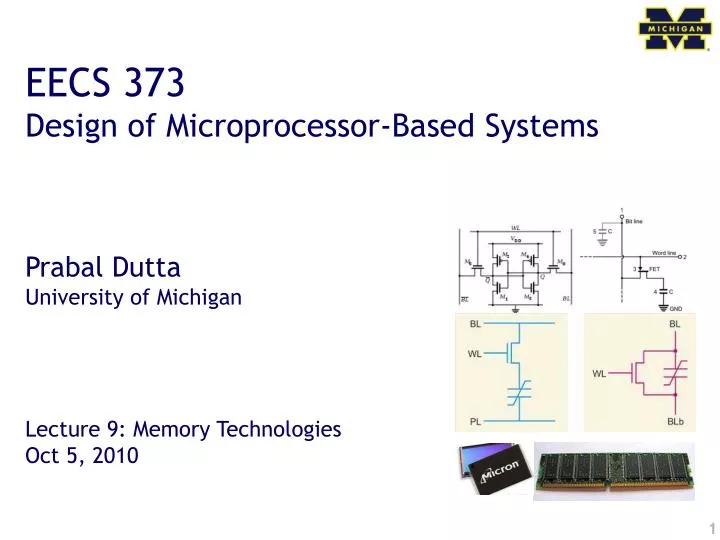
EECS 373 Design of Microprocessor-Based Systems Prabal Dutta University of Michigan Lecture 9: Memory Technologies Oct 5, 2010. Announcements. Homework #1 Due on Thursday, 10/7, beginning of class Comments? Questions? Office hours Tue, 10/5, 2:30 PM to 4:00 PM, EECS 2334

E N D
EECS 373 Design of Microprocessor-Based Systems Prabal Dutta University of Michigan Lecture 9: Memory Technologies Oct 5, 2010
Announcements • Homework #1 • Due on Thursday, 10/7, beginning of class • Comments? Questions? • Office hours • Tue, 10/5, 2:30 PM to 4:00 PM, EECS 2334 • Mid-semester feedback • Should get an email with instructions • Fill out online in Wolverine Access • Helps us to improve the class • Update on mid-course corrections…
Course corrections:What was asked for What has been done • Enable more inter-student interaction Created IRC channel • channel #eecs373 on irc.freenode.net • http://nuclear.eecs.umich.edu/irclogs/irclogger_logs/eecs373 • Annotated roadmap to readings roadmap.html added to syllabus • More homework HW#1 was assigned; due on Thursday • More lab testing Trying, but hard to get full coverage • A “found bugs” page See “Lab Bug Website” on class homepage • Upload lecture notes Posting before class • More in-class exercises Working in more exercises during class
Outline • Minute quiz • Announcements • Memory Landscape • Memory Architecture • Non-volatile Memories • Volatile Memories
External memory attaches to the processor via the external memory controller and bus Atmel SAM3U
External memory bus transactions • Read and write transactions • Interfacing/handshaking • Timing constraints • Access speeds • Wait states
Interface and architecture of external memory devices • A: 20-bit address bus • DQ: 8-bit data bus • CE#: chip enable • WE#: write enable • OE#: output enable
Basic categories of memory • Read-Only Memory (ROM) • Can only be read (accessed) • Cannot be written (modified) • Contents are often set before ROM is placed into the system • Random-Access Memory (RAM) • Can be read/written • Term used for historical reasons • Technically, ROMs are also random access • Volatile memory • Loses contents when power is lost • Often stores program state, stack, and heap • In desktop/server systems, also stores program executable • Non-volatile memory • Retains contents when power is lost • Used for boot code in almost every system
Choosing the right memory requires balancing many tradeoffs • Volatility: need to retain state during power down? • Cost: wide range of absolute $ and $/bit costs • Organization: 64Kbx1 or 8Kbx8? • Interface • Serial or serial or parallel or parallel or parallel? • Synchronous or asynchronous? • Access times: critical for high-performance • Modify times: critical for write-intensive workloads • Erase process: at wire-line speed or 5 minutes in UV? • Erase granularity: word, page, sector, chip?
Outline • Minute quiz • Announcements • Memory Landscape • Memory Architecture • Non-volatile Memories • Volatile Memories
Internal organization of memory is usually an array Mem Cell Mem Cell Mem Cell Mem Cell word lines • Different memory • types (e.g. SRAM vs • DRAM) are • distinguished by the • technology used to • implement the • memory cell, e.g.: • SRAM: 6T • DRAM: 1T/1C Mem Cell Mem Cell Mem Cell Mem Cell Mem Cell Mem Cell Mem Cell Mem Cell Mem Cell Mem Cell Mem Cell Mem Cell What should be the aspect ratio (# rows vs #cols)? bit lines
Physical (on-chip) memory configuration • Physical configurations are typically square • Square minimizes length of (word line + bit line) • Shorter length means • Shorter propagation time • Faster data access • Smaller trc (read cycle time) • Exercise: Assume n2 memory cells configured as • n-by-n square array. What is the worst case delay? • n2-by-1 rectangular. What is the worst case delay? • Exercise: Does wire length dominate access time? • Assume propagation speed on chip is 2/3 c (2x10^8 m/s) • Assume 1Mbit array is 1 cm x 1 cm
Logical (external) memory configuration • External configurations are tall and narrow • More address lines (12 to 20+, typically) • Fewer data lines (8 or 16, typically) • The narrower the configuration • The greater the pin efficiency • Adding one address pin cuts data pins in half • The easier the data bus routing • Many external configurations for given capacity • 64 Kb = 64K x 1 (16 A + 1 D = 17 pins) • 64 Kb = 32K x 2 (15 A + 2 D = 17 pins) • 64 Kb = 16K x 4 (14 A + 4 D = 18 pins) • 64 Kb = 8K x 8 (13 A + 8 D = 21 pins) • 64 Kb = 4K x 16 (12 A + 16 D = 28 pins) • 64 Kb = 2K x 32 (11 A + 32 D = 43 pins)
Supporting circuitry is needed to address memory cell and enable reads and writes Memory Array 16 bits (4 x 4) A0 Control signals Select chip Select memory cell Control read/write Map internal array to external configuration (4x4 16x1) A1 2:4 decoder A2 A3 4:1 mux/demux OE# CS# WE# D0
Refresher on the memory-bus interface • Chip Select (CS#) • Enables device • Ignores all other inputs if CS# is not asserted • Write Enable (WE#) • Enables write tri-state buffer • Store D0 at specified address • Output Enable (OE#) • Enable read tri-state buffer • Drive D0 with value at specified address
Outline • Minute quiz • Announcements • Memory Landscape • Memory Architecture • Non-volatile Memories • Volatile Memories
Mask ROM word lines • The “simplest” memory technology • Presence/absence of diode at each cell denote value • Pattern of diodes defined by mask used in fab process • Contents are fixed when chip is made; cannot be changed • High upfront setup costs (mask costs) • Small recurring marginal costs • Good for applications where • Cost sensitivity drives design • Upgrading contents not an issue • e.g. boot ROM, CPU microcode • Exercise: • What “value” does a diode encode? • What are the contents: • Where A<2:0> = 101? • Where A<2:0> = 110? Bit lines
EPROM • Erasable Programmable Read-Only Memory • Constructed from floating gate FETs • Charge trapped on the FG erases cell • High voltage (13V +) applied to the control gate • “Writes” the cell with a 0 • Allows FG charge to be dissipated • Erasing means changing form 0 1 • Uses UV light (not electrically!) • Electrons are trapped on a floating gate • Writing means changing from 1 0 • Erase unit is the whole device • Retains data for 10-20 years • Not used much these days • Costly because • Use of quartz window (UV transparent) • Use of ceramic package • PROM (or OTP) is same, just w/o window
Flash Memory • Electrically erasable (like EEPROM, unlike EPROM) • Used in many reprogrammable systems these days • Erase size is block (not word); can’t do byte modifications • Erase circuitry moved out of cells to periphery • Smaller size • Better density • Lower cost • Reads are like standard RAM • Can “write” bits/words (actually, change from 1 0) • Write cycle is O(microseconds) • Slower then RAM but faster than EEPROM • To (re)write from 0 1, must explicitly erase entire block • Erase is time consuming O(milliseconds to seconds) • Floating gate technology • Erase/write cycles are limited (10K to 100K, typically)
Outline • Minute quiz • Announcements • Memory Landscape • Memory Architecture • Non-volatile Memories • Volatile Memories
Static RAM • SRAMs are volatile • Basic cell • Bistable core • 4T: uses pullup resistors for M2, M4 • 6T: uses P-FET for M2, M4 • Access transistors • BL, BL# are provided to improve noise margin • 6T is typically used (but has poor density) • Fast access times O(10 ns) • Read/write speeds are symmetric • Read/write granularity is word
Dynamic RAM • Requires only 1T and 1C per cell • Outstanding density and low cost • Compare to the 6T’s per SRAM cell • Cost advantage to DRAM technology • Small charges involved relatively slow • Bit lines must be pre-charged to detect bits • Reads are destructive; internal writebacks needed • Values must be refreshed periodically • Prevents charge from leaking away • Complicates control circuitry slightly
Questions? Comments? Discussion?