Download
1 / 44
450 likes | 993 Views
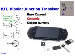
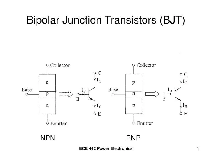
Bipolar Junction Transistors (BJT). NPN. PNP. BJT Cross-Sections. Emitter. Collector. NPN PNP. Common-Emitter NPN Transistor. Reverse bias the CBJ. Forward bias the BEJ. Input Characteristics. Plot I B as f(V BE , V CE )

E N D
Bipolar Junction Transistors (BJT) NPN PNP ECE 442 Power Electronics
BJT Cross-Sections Emitter Collector NPN PNP ECE 442 Power Electronics
Common-Emitter NPN Transistor Reverse bias the CBJ Forward bias the BEJ ECE 442 Power Electronics
Input Characteristics • Plot IB as f(VBE, VCE) • As VCE increases, more VBE required to turn the BE on so that IB>0. • Looks like a pn junction volt-ampere characteristic. ECE 442 Power Electronics
Output Characteristics • Plot IC as f(VCE, IB) • Cutoff region (off) • both BE and BC reverse biased • Active region • BE Forward biased • BC Reverse biased • Saturation region (on) • both BE and BC forward biased ECE 442 Power Electronics
Transfer Characteristics ECE 442 Power Electronics
Large-Signal Model of a BJT KCL >> IE = IC + IB βF = hFE = IC/IB IC = βFIB + ICEO IE = IB(1 + βF) + ICEO IE = IB(1 + βF) IE = IC(1 + 1/βF) IE = IC(βF + 1)/βF ECE 442 Power Electronics
Transistor Operating Point ECE 442 Power Electronics
DC Load Line VCC/RC VCC ECE 442 Power Electronics
BJT Transistor Switch ECE 442 Power Electronics
BJT Transistor Switch (continued) ECE 442 Power Electronics
BJT in Saturation ECE 442 Power Electronics
Model with Current Gain ECE 442 Power Electronics
Miller Effect iout vbe vce ECE 442 Power Electronics
Miller Effect (continued) ECE 442 Power Electronics
Miller Effect (continued) • Miller Capacitance, CMiller = Ccb(1 – A) • since A is usually negative (phase inversion), the Miller capacitance can be much greater than the capacitance Ccb • This capacitance must charge up to the base-emitter forward bias voltage, causing a delay time before any collector current flows. ECE 442 Power Electronics
Saturating a BJT • Normally apply more base current than needed to saturate the transistor • This results in charges being stored in the base region • To calculate the extra charge (saturating charge), determine the emitter current ECE 442 Power Electronics
The Saturating Charge • The saturating charge, Qs storage time constant of the transistor ECE 442 Power Electronics
Transistor Switching Times ECE 442 Power Electronics
Switching Times – turn on • Input voltage rises from 0 to V1 • Base current rises to IB1 • Collector current begins to rise after the delay time, td • Collector current rises to steady-state value ICS • This “rise time”, tr allows the Miller capacitance to charge to V1 • turn on time, ton = td + tr ECE 442 Power Electronics
Switching Times – turn off • Input voltage changes from V1 to –V2 • Base current changes to –IB2 • Base current remains at –IB2 until the Miller capacitance discharges to zero, storage time, ts • Base current falls to zero as Miller capacitance charges to –V2, fall time, tf • turn off time, toff = ts + tf ECE 442 Power Electronics
Charge Storage in Saturated BJTs Charge storage in the Base Charge Profile during turn-off ECE 442 Power Electronics
Example 4.2 ECE 442 Power Electronics
Waveforms for the Transistor Switch VCC = 250 V VBE(sat) = 3 V IB = 8 A VCS(sat) = 2 V ICS = 100 A td = 0.5 µs tr = 1 µs ts = 5 µs tf = 3 µs fs = 10 kHz duty cycle k = 50 % ICEO = 3 mA ECE 442 Power Electronics
Power Loss due to IC for ton = td + tr • During the delay time, 0 ≤t ≤td • Instantaneous Power Loss • Average Power Loss ECE 442 Power Electronics
During the rise time, 0 ≤t ≤tr ECE 442 Power Electronics
Average Power during rise time ECE 442 Power Electronics
Total Power Loss during turn-on ECE 442 Power Electronics
Power Loss during the Conduction Period ECE 442 Power Electronics
Power Loss during turn offStorage time ECE 442 Power Electronics
Power Loss during Fall time ECE 442 Power Electronics
Power Loss during Fall time (continued) ECE 442 Power Electronics
Power Loss during the off time ECE 442 Power Electronics
The total average power losses ECE 442 Power Electronics
Instantaneous Power for Example 4.2 ECE 442 Power Electronics
BJT Switch with an Inductive Load ECE 442 Power Electronics
Load Lines ECE 442 Power Electronics