Download
1 / 13
130 likes | 214 Views
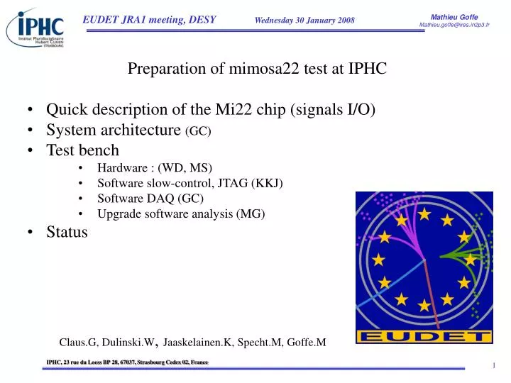
Preparation of mimosa22 test at IPHC Quick description of the Mi22 chip (signals I/O) System architecture (GC) Test bench Hardware : (WD, MS) Software slow-control, JTAG (KKJ) Software DAQ (GC) Upgrade software analysis (MG) Status.

E N D
Preparation of mimosa22 test at IPHC • Quick description of the Mi22 chip (signals I/O) • System architecture (GC) • Test bench • Hardware : (WD, MS) • Software slow-control, JTAG (KKJ) • Software DAQ (GC) • Upgrade software analysis (MG) • Status Claus.G, Dulinski.W, Jaaskelainen.K, Specht.M, Goffe.M
Input • Input clock : 100 MHz clock provided in LVDS by the digital auxiliary board.. • Slow control JTAG: for parameterization of bias, signal selection, pattern value & discriminator selection • Synchronization of the chip is done by two signals : START & SPEAK • Voltage and bias reference: (Some of these voltages can also be fix by JTAG) • Output • Data output • Mimosa 22 digital output => DAQ : The 128 columns are multiplexed to 16 digital output. With programmable pattern header • Mimosa 22 analog output => DAQ : There are 8 analog parallel output • Marker of Mimosa 22 : Each Matrices analog and digital have their own markers to pilot the DAQ. • DAC output (Bias test points) • Temperature sensor. Two diodes are implement to measure the temperature at the top and the bottom of the chip * Doc : « cartes_mi22_v1.2 » from gilles Claus
Temperature sensor DAC Bias outputs Signal Sync & JTAG Discri Threshold Markers 8 Analog outputs 4608 pixels Temperature sensor Voltage reference Clock LVDS CMOS 16 Digital outputs 73 728 pixels 17 differents type of pixels CLK_A, MK_SYNC_D, MK_TEST_D Matrice of 576 line by 136 columns CLK_D, MK_SYNC_D, MK_TEST_D
Architecture * Doc : « cartes_mi22_v1.2 » from gilles Claus
Hardware from DAQ side : • A digital interface card • It is a digital extension of acquisition imager board. It provide LVDS / CMOS conversion of the digital outputs of the matrices to be acquire by the cmos Imager_board input. It manage the distribution of the clock, synchro and markers signals between card
Sync signal JTAG Digital Data 15-12 To USB extension board DigitalData 11-8 DigitalData 7-4 Marker Digital DigitalData 3-0 Marker Analog Analog Output 12,1 mm Digital Auxiliary board Proimity board 4,1 mm Area of active matrice 2,53*10.59 mm Analog Auxiliary board
HARDWARE chip side Three board are needed to test the chip : • The proximity board where the chip is bound. It include the minimum front-end electronic, just the signal amplification for critical signals. • The Analog auxiliary board : To buffer the 8 analog signal of Mi22 in differential to be transmit in long distance ( 40 m ). We will use two AUX_V4 to do the acquisition of the 8 channels. • The Digital auxiliary board : it generate the 100 MHz clock of Mi22. Buffering the digital signals from DAQ to Mi22 ( and the JTAG ) and from Mi22 to DAQ in LVDS to be transmit in long distance ( 40 m ). It provide also power supply of the chip and proxi_board. * Doc : « cartes_mi22_v1.2 » from gilles Claus
Current Master Configuration file Number of MIMOSA22 devices on JTAG chain Selection of the device for independent parameter setup and visualization Add a device (Device Configuration ) to the Master Configuration Reload Device configuration from file Parallel Port Hardware address Setting Device Reset (by RSTB signal) Device Start (by using JTAG_Start bit in Romode0 register ) Write all the parameters to the device Write the DAC parameters to the device Read back Device Settings JTAG interface • Multiple Mi22 control • with independent JTAG • values for each chip
To modify Discriminator Control register values for MIMOSA22 device To modify Readout Mode register values for MIMOSA22 device To modify Bias register values for MIMOSA22 device To modify Column Control register values for MIMOSA22 device To modify Line Pattern register values for MIMOSA22 device Device parameters/registers
Software DAQ Adaptation of the software to manage N acquisition cards with different format of data. Here : Two analog and one digital card with different frequency and different number of pixels
Root monitoring under windows on the acquisition PC For the 8 analog columns CDS Raw Data Read Calib Hits For the digital part Discriminator
upgrade data analysis software:- For the laboratory tests, we will adapt the mimosa_analysis labview program to be able to analyze the 8 analog outputs of the chip and characterize the different sub matrices
Status February • PCB and component are ready (assembling soon) • Chip bounding (in nexts weeks) • Bench validation • Chip testing (starting in Mars) Validation of the acquisition system by emulating the mi22 chip output signal with a pattern generator