
Uploaded by
lumina
2 SLIDES
226 VIEWS
20LIKES
GND
DESCRIPTION
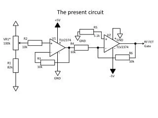
The present circuit. +5V. R5 5.1 k. U2. +. U1. +. R2 10k. VR1* 100k. GND. TLV2374. GND. RF FET Gate. +. +. R4 10k. TLV2374. -. -. -. -. R6 10k. R3 10k. R 1 82k. -5V. GND. Proposed measures. +5V. C1 0.1uF. R5 5.1 k. U2. +. U1. +. R2 10k. VR1* 100k. GND.
Download
1 / 2
Download Presentation 
GND
An Image/Link below is provided (as is) to download presentation
Download Policy: Content on the Website is provided to you AS IS for your information and personal use and may not be sold / licensed / shared on other websites without getting consent from its author.
Content is provided to you AS IS for your information and personal use only.
Download presentation by click this link.
While downloading, if for some reason you are not able to download a presentation, the publisher may have deleted the file from their server.
During download, if you can't get a presentation, the file might be deleted by the publisher.
E N D
Presentation Transcript
The present circuit +5V R5 5.1k U2 + U1 + R2 10k VR1*100k GND TLV2374 GND RF FET Gate + + R4 10k TLV2374 - - - - R6 10k R3 10k R1 82k -5V GND
Proposed measures +5V C1 0.1uF R5 5.1k U2 + U1 + R2 10k VR1*100k GND TLV2374 GND RF FET Gate + + R4 10k TLV2374 - - - - R6 10k R3 10k D1General Schottky Diode R1 82k -5V GND

More Related