Analogue Input/Output
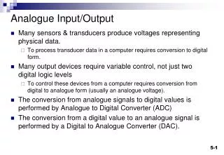
Analogue Input/Output. Many sensors & transducers produce voltages representing physical data. To process transducer data in a computer requires conversion to digital form. Many output devices require variable control, not just two digital logic levels

Analogue Input/Output
E N D
Presentation Transcript
Analogue Input/Output • Many sensors & transducers produce voltages representing physical data. • To process transducer data in a computer requires conversion to digital form. • Many output devices require variable control, not just two digital logic levels • To control these devices from a computer requires conversion from digital to analogue form (usually an analogue voltage). • The conversion from analogue signals to digital values is performed by Analogue to Digital Converter (ADC) • The conversion from a digital value to an analogue signal is performed by a Digital to Analogue Converter (DAC).
DA Converter DAC function Parallel DAC Analogue output n bit value VAgnd Vref Serial DAC would typically have a single data input line and a clock input signal which would be used to clock in the serial data stream. Adv. : - Fewer pins. Disadv. : Slower data transfer.
Analogue Output • Digital to Analogue Converter (DAC) • DAC Characteristics • resolution = 1/2n where n is the number of bits • Max. digital value = 2n – 1 • output voltage range – determined by reference voltage (Vref and AGND) • Step size in volts = resolution x voltage range • Max output voltage = (2n – 1)/ 2n x voltage range • uni-polar / bipolar types • slew rate – rate of change of output. • interface – parallel (fast) or serial (slower but uses fewer connections)
d1 d3 d2 d0 DAC principles – Example 4-bit DAC • Sum currents with operational amplifier R 2R Vref/2 1 Vo = - Vref(Rf/Rinput) 4R Vref/4 0 - Vo 8R Vref/8 + 1 Vo = -(Vref-AGND)(digital value/2n) Vo α digval/ 2n 16R Vref/16 AGND 1 Example: with 4-bit value = 1011 Vo = -Vref(d3/2 + d2/4 + d1/8 + d0/16) Vo = -Vref(1/2 + 1/8 + 1/16) Vo = -Vref(11/16) Vref
Output from DAC Output Voltage VMAX = Maximum output voltage where n is number of bits MAXVAL = Maximum digital value = 2n -1 where n is number of bits VMAX Digital Value MAXVAL
Example DAC device • M AX5722 dual,12-bit, low-power, buffered voltage output, digital-to-analog converter (DAC) is packaged in a space-saving 8-pin μMAX package (5mm ✕ 3mm). Ultra-Low Power Consumption 112μA at VDD = +3.6V 135μA at VDD = +5.5V Wide +2.7V to +5.5V Single-Supply Range 8-Pin μMAX Package 0.3μA Power-Down Current Guaranteed 12-Bit Monotonicity (±1LSB DNL) Safe Power-Up Reset to Zero Volts at DAC Output Three Software-Selectable Power-Down Impedances (100kΩ, 1kΩ, Hi-Z) Fast 20MHz, 3-Wire SPI, QSPI, and MICROWIRECompatible Serial Interface Rail-to-Rail Output Buffer Amplifiers Schmitt-Triggered Logic Inputs for Direct Interfacing to Optocouplers Wide -40°C to +125°C Operating Temperature Range
Audio & LPC 23xx DAC example • Recreate audio • What resolution? • What sampling rate ?
Analogue Input • Analogue to Digital Converter (ADC) • ADC Characteristics • resolution = 1/2n where n is the number of bits • Max. digital value = 2n – 1 • input voltage range – determined by the reference voltages (Vref and AGND) • Step size in volts = resolution x voltage range • uni-polar / bipolar types • interface – parallel (fast) or serial (slower but uses fewer connections) • often integrated into microcontrollers.
Converter Analogue input n bit result VAgnd Vref General ADC function • The analogue input voltage is converted into a value. • The value is dependent on the reference voltages and the number of bits n.
Analogue Input • Main types (i.e.methods) of ADC • Successive approximation – good all-rounder • Flash – fastest type • Sigma-delta – good for audio • Dual slope integrating – slow but high resolution with good noise immunity • others – Sampling, ramp, charge balancing • Characteristics • resolution • conversion method • conversion time • input voltage range • interface – parallel (fast) or serial(fewer connections)
MCP3208 • Features 12-bit resolution ± 1 LSB max DNL ± 1 LSB max INL (MCP3204/3208-B) ± 2 LSB max INL (MCP3204/3208-C) 4 (MCP3204) or 8 (MCP3208) input channels Analog inputs programmable as single-ended or pseudo-differential pairs On-chip sample and hold SPI serial interface (modes 0,0 and 1,1) Single supply operation: 2.7V - 5.5V 100 ksps max. sampling rate at VDD = 5V 50 ksps max. sampling rate at VDD = 2.7V Low power CMOS technology: 500 nA typical standby current, 2 μA max. 400 μA max. active current at 5V Industrial temp range: -40°C to +85°C Available in PDIP, SOIC and TSSOP packages
Example:8-bit ADC with Vref +5v and 0v VAgnd • Number of steps (values) = 2n = 28 = 256 • steps are numbered 0 to 255 • step size = reference voltage range / number of steps = (5v – 0v) / 256 = 19.53125 x10⁻³v 20mv • number range 0 to 255 corresponds to voltage range of 0 to 5v • ADC value = (Vin / (Vref – Agnd)) * 256 : remember max ADC value is 255 so max input voltage that can be converted accurately is less than 5 volts. • What is the maximum convertible input voltage?
4 3 2 1 V 50mv 10mv 30mv 70mv 20mv 40mv 60mv 8-bit ADC with 5v reference ADC value 255 ADC value 0 Volts 4.98
Cont. ADC value 4 3 2 1 Volts 0 10mv 30mv 50mv 70mv 20mv 40mv 60mv 80mv
Quantization Error Each input sample is assigned a quantization interval that is closest to its amplitude height. If an input sample is not assigned a quantization interval that matches its actual height, then an error is introduced into the conversion process. This error is called quantization error/noise.
Reducing quantization error • One way to reduce quantization noise is to increase the amount of quantization intervals. • The difference between the input signal amplitude height and the quantization interval decreases as the quantization intervals are increased (increases in the intervals decrease the quantization noise). • Solved by increasing the ADC resolution (number of bit) in proportion to the increase in quantization intervals. 8 7 6 5 4 3 2 1 0
Analogue Input Example • Example - The LM35 series are precision integrated-circuit temperature sensors, whose output voltage is linearly proportional to the Celsius (Centigrade) temperature.
LM35 & LPC23xx Interface Example • ADC range (LPC23xx) 0V to + 3.3 V • LM35 Linear + 10.0 mV/°C scale factor • Use a basic Centigrade temperature sensor +2°C to +150°C • Max voltage from sensor = 10mV×150 = 1.5V Scale the input voltage accordingly to match input the range of the ADC
LM35 & LPC23xx Interface Example • step size = reference voltage range / number of steps = (3.3v – 0v) / 1024 = 3.22265625 x10⁻³v • Every 1°C is now equivalent to 20.0 mV • Temperature resolution > 0.2°C AI0 LPC23xx
ADC input • Good practice to • Limit the voltage range (input protection) • Filter the signal From sensor To ADC input
Conversion Control Interrupt request Busy Mut iplexer Result Register Start conversion AN0 Sample & Hold AN1 Converter VAREF VAGND ANn ADC Block diagram Interface to uP Reference voltage
ADC – principle of operation • The voltage is presented to the ADC input. • The ADC is sent a signal to start conversion • While the conversion takes place the input voltage should remain stable. • The ADC outputs a signal to indicate that it is busy doing the conversion and should not be disturbed. • When the conversion is completed the ADC makes the result available and outputs a signal to indicate that the conversion has completed (e.g remove the busy signal)
Multiplexer and Sample/Hold • To convert several analogue inputs • use an ADC for each input or more usually … • use one ADC and switch the inputs through a multiplexer • requires selection of input before each conversion is started and a short delay is required before conversion started to allow switching to occur and signal to settle. • Sample and Hold (S&H) • while conversion takes place voltage must remain stable • sample voltage – input connected to S&H • voltage held on a capacitor • sample time – charging time of capacitor • input signal disconnected from S&H
Summary • Analogue inputs are often required in embedded applications and so ADCs are integrated into most microcontrollers (DACs less so) • ADCs and DAC also exist as standalone IC devices - often specialist devices e.g. High speed or high resolution ADCs, fast DACs for video output. • Main characteristics of interest is • resolution - number of bits • voltage range • ADC - conversion time • DAC - slew rate
ADC on the LPC23xx • LPC23xx ADC Features • 10 bit successive approximation analogue to digital converter. • Input multiplexing among 6 pins or 8 pins. • Power down mode. • Measurement range 0 to 3.3 V. • 10 bit conversion time ≥ 2.44 μs. • Burst conversion mode for single or multiple inputs. • Optional conversion on transition on input pin or Timer Match signal. • Individual result registers for each A/D channel to reduce interrupt overhead.
Using the ADC • The ADC like all other peripherals is accessed through a group of associated registers. (see pages 575ff of the user manual for a detailed description) • As an example we will look at the A/D Control Register (AD0CR)
AD0CR 0- Conversions are software controlled and require 11 clocks. 1- The AD converter does repeated conversions at the rate selected by the CLKS field, scanning (if necessary) through the pins selected by 1s in the SEL field. The first conversion after the start corresponds to the least-significant 1 in the SEL field, then higher numbered 1 bits (pins) if applicable. Repeated conversions can be terminated by clearing this bit, but the conversion that’s in progress when this bit is cleared will be completed. Selects which of the AD0.7:0 pins is (are) to be sampled and converted. For AD0, bit 0 selects Pin AD0.0, and bit 7 selects pin AD0.7. In software-controlled mode, only one of these bits should be 1. In hardware scan mode, any value containing 1 to 8 ones. All zeroes is equivalent to 0x01. This bit is significant only when the START field contains 010-111. In these cases:1- Start conversion on a falling edge on the selected CAP/MAT signal. 0 Start conversion on a rising edge on the selected CAP/MAT signal 1 The A/D converter is operational. 0 - The A/D converter is in power-down mode. This field selects the number of clocks used for each conversion in Burst mode, and the number of bits of accuracy of the result in the LS bits of ADDR, between 11 clocks (10 bits) and 4 clocks (3 bits). 000 11 clocks / 10 bits 001 10 clocks / 9 bits 010 9 clocks / 8 bits 011 8 clocks / 7 bits 100 7 clocks / 6 bits 101 6 clocks / 5 bits 110 5 clocks / 4 bits 111 4 clocks / 3 bits The APB clock (PCLK) is divided by (this value plus one) to produce the clock for the A/D converter, which should be less than or equal to 4.5 MHz. Typically, software should program the smallest value in this field that yields a clock of 4.5 MHz or slightly less, but in certain cases (such as a high-impedance analog source) a slower clock may be desirable. When the BURST bit is 0, these bits control whether and when an A/D conversion is started: 000 No start (this value should be used when clearing PDN to 0). 001 Start now. 010 Start when the edge selected by bit 27 occurs on P2.10/EINT0. 011 Start when the edge selected by bit 27 occurs on P1.27/CAP0.1. 100 Start when the edge selected by bit 27 occurs on MAT0.1. 101 Start when the edge selected by bit 27 occurs on MAT0.3[1]. 110 Start when the edge selected by bit 27 occurs on MAT1.0. 111 Start when the edge selected by bit 27 occurs on MAT1.1. R = Reserved, user software should not write or read ones to reserved bits.
AD0CR AD0CR = ( 0x01 << 0 ) | /* SEL=1,select channel 0~7 on ADC0 */ ( ( Fpclk / ADC_Clk - 1 ) << 8 ) | /* CLKDIV = Fpclk / 1000000 - 1 */ ( 0 << 16 ) | /* BURST = 0, no BURST, software controlled */ ( 0 << 17 ) | /* CLKS = 0, 11 clocks/10 bits */ ( 1 << 21 ) | /* PDN = 1, normal operation */ ( 0 << 24 ) | /* START = 0 A/D conversion stops */ ( 0 << 27 ); /* EDGE = 0 (CAP/MAT singal falling,trigger A/D conv */
Enable the ADC input pins • Before using the ADC the appropriate pins must be set as ADC inputs. This is accomplished using the PINSEL register(s) PINSEL1 |= 0x00004000; // Select only ADC channel 0
Reading the ADC • See example programs!
Example question • A 5 bit ADC is used to encode an analogue signal in the range 0V to +5V for linear PCM encoding determine: • The step size • Calculate the percentage resolution • Calculate the dynamic range in dB • Calculate the input voltage level corresponding 10110.
Solution • The step size • 2. Calculate the percentage resolution
Solution • 3 Calculate the dynamic range in dB • 4 Calculate the input voltage level corresponding 10110
Signal Energy Distribution for Human Speech 3,400 Hz 20 kHz 0 Hz 300 Hz Voice signal Bandpass Filtering Bandwidth (3.1 kHz) The human voice can produce sounds up to 20 kHz, but most sound is between 300 Hz and 3.4 kHz.The bandpass filter only passes this sound to reduce bandwidth.