GLAST Tracker
GLAST Tracker. Chuzenji lake. Kegon fall. Woodblock print by Hasui Kawase. Outline. Overview of GLAST Tracker. Requirements. Mechanical and electronics design. Production. Alignment. Production issues. Performance. Bad strips, hit efficiencies. TOT calibrations.

GLAST Tracker
E N D
Presentation Transcript
GLAST Tracker Chuzenji lake Kegon fall Woodblock print by Hasui Kawase
Outline • Overview of GLAST Tracker. • Requirements. • Mechanical and electronics design. • Production. • Alignment. • Production issues. • Performance. • Bad strips, hit efficiencies. • TOT calibrations. • Threshold, trigger dispersions. • Transient noise issues. • Current Status and Future Schedule.
Gamma-ray Large Area Space Telescope GLAST/LAT Collaboration Stanford University & Stanford Linear Accelerator Center NASA Goddard Space Flight Center Naval Research Laboratory University of California at Santa Cruz Sonoma State University University of Washington Texas A&M University – Kingsville Ohio State University Commissariat a l’Energie Atomique, Saclay Ecole Polytechnique, College de France, CENBG (Bordeaux) Hiroshima University Institute of Space and Astronautical Science University of Tokyo Instituto Nazionale di Fisica Nucleare Agenzia Spaziale Italiana Instituto di Fisica Cosmica, CNR Royal Institute of Technology, Stockholm Stockholms Universitet
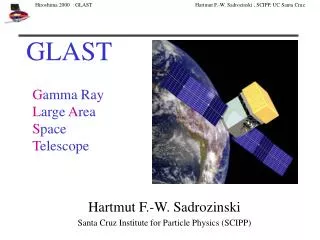
e– e+ GLAST/LAT Overview • Satellite experiment to observe gamma-try from Universe. • Wide energy range: 20 MeV – 300 GeV • Large effective area: > 8000 cm2 (5xEGRET) • Wide field of view: > 2 sr (4xEGRET) • Scientific objectives. • Dark matter. • Neutralino annihilation. • Particle acceleration. • Cosmic ray origin • Pair-conversion telescope. • “Clear” signature. • Background rejection.
Instrument Configuration • Tracker: conversion, tracking. • Angular resolution is dominated by scattering. • Converter thickness optimization. • Calorimeter: energy measurement. • 8.4 radiation length. • Use shower development to compensate for the leak. • Anti-coincidence detector: • Efficiency > 99.97%. Si Tracker 90 m2 , 228 µm pitch ~0.9 million channels g e- e+ Anti-coincidence Detector Segmented scintillator tiles 99.97% efficiency CsI Calorimeter 8.4 radiation length
Requirements for Tracker • Conversion Efficiency > 58%. • Aspect (H/W) ratio < 0.45 (for wide field of view). • Active area > 19,000 cm2 (Fraction > 88%). • 6-in-a-row tracker trigger. • Efficiency > 90%. • Single layer trigger rate < 50 kHz. • Trigger jitter < ±300 ns for Q > 0.5 MIP. • Threshold dispersion < 10%. • Noise data volume: 40 noise hits per event. • Average Noise occupancy < 5x10⁻⁵ . • Hit efficiency > 98% • Dead time < 10% for 10 kHz. • Power consumption < 160 W. • Survival temperature range: -15 – 45 °C. Careful for what you wish in NASA project.
Mechanical Design Multi-Chip Electronics Module (MCM) “Thin” Tungsten Foil (3% X0) 12 Locations Silicon Strip Detectors 18 X-Y Pairs of Planes 19 Carbon-Fiber Tray Panels 18 Y 17 X Carbon-Fiber Sidewalls (Aluminum covered) 16 Y 5 type of trays. 4 Y 2 mm gap 3 X 2 Y 1 X 0 Y “Thick” Tungsten Foil (18% X0) 4 Locations No Tungsten Foil 2 Locations Readout Cable Titanium Flexure Mounts
Microbonding Tray Structure Silicon Strip Detectors Structural tray panel: C-C machined closeout frame Aluminum honeycomb core CFRP face sheets Wire Bonds Bias Plane Multi-Chip Module Bottom Layer Tungsten Foil Multi-Chip Module Top Layer
Readout Electronics Architecture • Emphasis on compactness, minimum of wiring, and redundancy: • Serial, LVDS readout and control lines on flat flex-circuit cables. • Any single component (GTFE, GTRC, cable) can fail without affecting the other. • GLAST Tracker Readout Controller (GTRC) • 9 GTRC per cable. • Communication between 24 GTFE and back-end electronics. • TOT measurement from layer-OR trigger signal
Tracker Front-end Electronics • GTFE (GLAST Tracker Front-end Electronics) ASIC • Preamplifier - shaper - discriminator • One threshold DAC and one calibration DAC per chip. • 64 channels per chip, 24 chips per MCM. • Noise: ~1500 e for 4 SSD ladder. • Gain: ~100 mV/fC. • Peaking time: 1.5 µs. • 0.1 mW/channel. GTFE GTRC
SSD 8.95 cm x 8.95 cm. 226 µm pitch. 400 µu thick. Manufactured by HPK. 10,368 wafers. 0.5% rejection fraction. 2.5 µm dicing accuracy. INFN/Pisa 8.95 cm SSD reference crosses 8.95 cm
Ladder and Tray Assembly • Ladder Assembly • Take advantage of excellent dicing accuracy. • Manual alignment. • Precise SSD alignment within ladder. • No CMM required. • Tray Assembly • 20 µm ladder placement accuracy. INFN/Pisa
Tower Assembly Attach cables Stacking trays ~1m Side panel 8 type of cables due to space constraint Alignment pin
horizontal displacement: 157m vertical displacement: 81m Tray Alignment by Muon Track real position θ X4 X3 X2 X1 X0 ideal position res = x + z · cot(θ) INFN/Pisa Data after alignment MC rms = 124 mm rms = 137 mm Scattering dominant Residual Residual
Production Issues • Delamination due to thermal-vacuum cycles. • Kapton bias circuit. • Extremely difficult to glue tungsten. • Polymer coating of tungsten. • Wire-bonding encapsulation. • Silicone contamination from pitch-adapter bonding process. • Eliminate use of silicone based tape. • SSD movement due to CTE mismatch of tungsten foil. • Eliminate encapsulation for SSD wire-bonding. • Reduce thermal excursion. • Pitch-adapter cracking. • Silent modification of Ni plating process. • Flex circuit delivery delays. • Incompetent vender. Pitch-adapter flex bonded over radius Kapton Bias Circuit ASIC MCM PWB Adhesive
Flight Module Delivery • All flight modules are delivered and integrated. • Flex cable delivery has been bottle neck. • ACD is being integrated. Total Monthly
Hot and Dead Strips • Hot strip definitions. • Data mask. • Mask noisiest strips to satisfy 5x10⁻⁵ average occupancy. • 7 masked strips. • Trigger mask. • Mask noisiest strips to satisfy 50 kHz layer trigger rate. Hot strips Mean: 0.7 / layer Dead strips Mean: 0.8 / layer 1% 1%
Disconnected Strips. • Disconnected Strips. • Broken pitch adapter. • Disconnected wire-bond between MCM and SSD. • Disconnected wire-bond between SSDs. Disconnected strips Mean: 3.0 / layer Broken ladder strips Mean: 4.4 / layer 1% 1%
Hit Efficiencies • Specification: hit efficiency > 98%. • 99.0% of layers satisfy the specification. • Average efficiency: 99.6%. 2%
TOT/Calibration DAC Calibration • TOT gain is calibrated for each channel. • Use MIP signals to calibrate “calibration” DAC. ~30% rms With gain correction Without gain correction ~8% rms
Trigger Jitter • Trigger jitter important for ACD veto. • Trigger time walk due to input charge is dominant source of trigger jitter. • Specification: Trigger jitter < ±0.3 µs for Q > 0.5 MIP. • Proper threshold setting necessary. Trigger timing for 0.5MIP Specification
~2 µs Threshold Dispersion • Trigger threshold. • Threshold at pulse peak. • Dispersion: 5.9%. (within chip: 5.2%, chip-to-chip: 2.7%). • Threshold for data capture. • Strip data is captured ~2 µs after trigger request. • Larger dispersion due to variation of fall time. • Dispersion: 12.0%. (within chip: 8.3%, chip-to-chip: 7.0%).
Transient Noise Issue • 6 layers out of 612 layers exhibit transient noise. • Infrequent (0/day – a few/hour). • Confined within one ladder. • Noisy ladder different episode to episode. • Many strips are affected at the same. • No apparent dependence on bias voltage or vacuum. • No major effect on operation. • Trigger rate, occupancy within specification on ground. Strip profile Occupancy time profile Layer-OR time profile
Current Status and Future Schedule • All flight detector modules are delivered. • Tracker meet all specifications. • DAQ integration and online software test. • Now – Jan 2006. • Environmental test at NRL. • Feb – June 2006. • Beam test at CERN(?) • Spare modules. • Proposal in preparation. • ~ June 2006. • Space craft integration. • Launch from Kennedy SFC. • Sep 2007. • Largest Silicon Detector in the Space. Spitzer Telescope Launch on a Delta II Heavy (near Earth)

