Download
1 / 4
40 likes | 169 Views
Exam Digital Design . August 2, 2002; 09:00 - 12:00 a.m. Problem 1. Use a Karnaugh map to minimize the following SOP expression: B’C’D’ + A’BC’D’ + ABC’D’ + A’B’CD + AB’CD + A’B’CD’ + A’BCD’ + ABCD’ + AB’CD’.

E N D
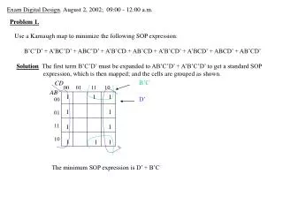
Exam Digital Design. August 2, 2002; 09:00 - 12:00 a.m. Problem 1. Use a Karnaugh map to minimize the following SOP expression: B’C’D’ + A’BC’D’ + ABC’D’ + A’B’CD + AB’CD + A’B’CD’ + A’BCD’ + ABCD’ + AB’CD’ Solution The first term B’C’D’ must be expanded to AB’C’D’ + A’B’C’D’ to get a standard SOP expression, which is then mapped; and the cells are grouped as shown. B’C CD 00 01 11 10 AB 1 1 1 1 1 1 1 1 1 1 D’ 00 01 11 10 The minimum SOP expression is D’ + B’C
Inputs Outputs X Y Z A B C D 0 0 0 0 1 0 0 0 0 1 1 1 1 1 0 1 0 1 0 1 1 0 1 1 0 1 0 1 1 0 0 1 0 1 0 1 0 1 0 0 0 1 1 1 0 1 1 1 0 1 1 1 0 1 1 1 Problem 2. The following is the truth table of a three-input, four-output combinational circuit. Obtain a PAL programming table for the circuit, and the PAL connection map. Solution PTERM INPUTS X Y Z A YZ’ 1 - 1 0 - X’Y’Z 2 0 0 1 - XZ’ 3 1 - 0 - X’Y’ 4 0 0 - - YZ 5 - 1 1 - XY 6 1 1 - - A 7 - - - 1 XY 8 1 1 - - - 9 - - - - Z 10 - - 1 - X’Y 11 0 1 - - - 12 - - - -
Problem 3. Specify the 17-bit control word that must be applied to the processor given in Figure 7-19 of Mano’s book to implement each of the following micro-operations: (a) R1 R2 + R6 (b) R3 Data in (c) R4 sl R3 (d) R6 R4 - Constant in (e) R3 R2 R7 (f) R7 0 (g) R1 R0 + 1 (h) R2 srR3 Solution DA AA BA MB FS MD RW (a) 001 010 110 0 00010 0 1 (b) 011 --- --- - ------- 1 1 (c) 100 --- 011 0 11000 0 1 (d) 110 100 --- 1 00101 0 1 (e) 011 010 111 0 01100 0 1 (f) 111 000 000 0 01100 0 1 (g) 001 000 --- 0 00001 0 1 (h) 010 --- 011 0 10100 0 1
15 14 13 12 11 10 9 8 7 6 5 4 3 2 1 0 0 1 Operation code Destination Source re- register (DR) gister(SB) AR10 00000111 R8 M[PC], PC PC + 1 SA AR11 10000111 R8 M[ R8 ] AR12 01000111 R[DR] R[SB] + R8 To IF Problem 4. Specify an instruction format for the micro-programmed computer that performs the operation R[DR] R[SB] + M[SA] Find the ASM chart for implementing the instruction you have found, assuming that the opcode is 0000111 (See Figure 8-24 in Mano’s book). List the sequence of micro-operations for executing this instruction, including the handling of the CAR values. Solution NA MS MC IL PI PL TD TA TB MB FS MD RW MM MW 135 NXT NXA NLI NLP LDP R8 -- -- Register -- Data In WR PC NW 71 CNT ----- NLI NLP NLP R8 R8 -- Register -- Data In WR Address NW 192 NXT NXA NLI NLP NLP DR R8 SB Register A+B FnUt WR -- NW