Download
1 / 1
10 likes | 178 Views
Introduction. Experiment. Theoretical Background. Experiment. 4 th Dr. Mow Shiah Lin Scholarship Award. Strain/Stress and Defects Analysis in Silicon Carbide. Ning Zhang and Michael Dudley Department of Materials Science and Engineering, Stony Brook University. Strain/Stress Mapping.

E N D
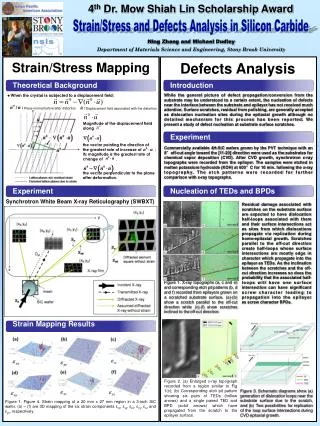
Introduction Experiment Theoretical Background Experiment 4th Dr. Mow Shiah Lin Scholarship Award Strain/Stress and Defects Analysis in Silicon Carbide Ning Zhang and Michael Dudley Department of Materials Science and Engineering, Stony Brook University Strain/Stress Mapping Defects Analysis While the general picture of defect propagation/conversion from the substrate may be understood to a certain extent, the nucleation of defects near the interface between the substrate and epilayer has not received much attention. Surface scratches, residual from polishing, are generally accepted as dislocation nucleation sites during the epitaxial growth although no detailed mechanism for this process has been reported. We present a study of defect nucleation at substrate surface scratches. • When the crystal is subjected to a displacement field: Plane normal before/after distortion Displacement field associated with the distortion Magnitude of the displacement field along . the vector pointing the direction of the greatest rate of increase of ; its magnitude is the greatest rate of change of . Commercially available 4H-SiC wafers grown by the PVT technique with an 8°off-cut angle toward the [11-20] direction were used as the substrates for chemical vapor deposition (CVD). After CVD growth, synchrotron x-ray topographs were recorded from the epilayer. The samples were etched in molten potassium hydroxide (KOH) at 600°C for 10 min. following the x-ray topography. The etch patterns were recorded for further comparison with x-ray topographs. the vector perpendicular to the plane after deformation. Nucleation of TEDs and BPDs Synchrotron White Beam X-ray Reticulography (SWBXT) Residual damage associated with scratches on the substrate surface are expected to have dislocation half-loops associated with them and their surface intersections act as sites from which dislocations propagate via replication during homo-epitaxial growth. Scratches parallel to the off-cut direction create half-loops whose surface intersections are mostly edge in character which propagate into the epilayer as TEDs. As the inclination between the scratches and the off-cut direction increases so does the probability that the associated half-loops will have one surface intersection can have significant screw character leading to propagation into the epilayer as screw character BPDs. Figure 1. X-ray topographs (a, c and e) and corresponding etch pit patterns (b, d and f) recorded from epilayers grown on a scratched substrate surface. (a)-(b) show a scratch parallel to the off-cut direction while (c)-(f) show scratches inclined to the off-cut direction. Strain Mapping Results Figure 2. (a) Enlarged x-ray topograph recorded from a region similar to Fig 1(c); (b) Corresponding etch pit pattern showing six pairs of TEDs (hollow arrows) and a single paired TED and BPD (solid arrows) which have propagated from the scratch to the epilayer surface. Figure 3. Schematic diagrams show (a) generation of dislocation loops near the substrate surface due to the scratch, and (b) Two possibilities for replication of the loop surface intersections during CVD epitaxial growth. Figure 1. Figure 4. Strain mapping of a 20 mm x 27 mm region in a 3-inch SiC wafer. (a) – (f) are 3D mapping of the six strain components εxx, εyy, εzz, εxy, εxz and εyz, respectively.