Download
1 / 1
10 likes | 212 Views
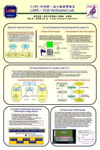
VLSI Design. EDA Tools. ADC & control. ADC & control. ADC & control. ADC & control. ADC & control. Circuit Model. expected response. test patterns. =. not equal !. faulty response. a chip with defects inside. Question: Where are the fault locations ?. Chip. RTL Code.

E N D
VLSI Design EDA Tools ADC & control ADC & control ADC & control ADC & control ADC & control Circuit Model expected response test patterns = not equal ! faulty response a chip with defects inside Question: Where are the fault locations ? Chip RTL Code RTL Simulation Results CMOS Image Sensor Design Nanometer SRAM Design Power Estimation BISG & Fault Diagnosis Analog Components Logic Sub-systems Embedded Memories quick synthesis ToggleFinder 3.82 % netlist Toggle count SPICE Quick SPICE Simulation Static or Logic Simulation Quick SPICE Model-Based cell expansion or physical design 3 % PowerMixer Feasible Inaccurate Too slow Feasible schematic or even layout Total power LARC 研究群 – 晶片驗證實驗室 LARC – VLSI Verification Lab. 指導老師:清華大學電機系 黃錫瑜 副教授 辦公室: 資電館 818 室 E-mail: syhuang@ee.nthu.edu.tw Research Topics At a Glance (1) Fault Diagnosis Tool Development for Logic IC’s Problem of Fault Diagnosis A New Paradigm for Scan Chain Diagnosis Our research is mainly in the areas of VLSI design, Testing, and Electronic Design Automation (EDA). (1) For VLSI design, we focus on Nanometer SRAM design and CMOS image sensor design. (2) For VLSI testing, weare working on Built-In Speed Grading (BISG) and fault diagnosis (3) For EDA, we are developing tools for efficient average and peakpower estimation Scan chains have been popularly used as the channels for silicon testing and debugging. We have developed a more versatile model-free paradigm for locating the faulty flip-flops in a scan chain by a number of signal processing techniques, such as filtering and edge detection. Fault diagnosis is to locate the defects in a failing IC. It is an important pre-processing step to guide the failure analysis process of an IC so as to improve the manufacturing yield. • Limitations of Existing Methods • (1) More or less bound to certain fault models • (2) Not suitable for bridging faults • (3) Not suitable for intermittent faults • Our contributions • Use signal processing techniques • Free of fault models • Good for stuck-at, transition, bridging, etc. • Works well when the fault is intermittent • Can be applied to hold-time faults (2) Power Estimation for Complex Logic IC’s • The power estimation is to predict the power consumption of an IC. It is important for battery lifetime estimation, thermal analysis for packaging and signal integrity analysis. Existing methods for power estimation have certain limitations such as inadequate accuracy and/or too time-consuming. In this research, we have developed an integrated prototype system consisting of two sub-program: • ToggleFinder: which can calculate the total switching activities inside a given RTL code without time-consuming gate-level simulation. • (2) PowerMixer: which can translate a certain amount of switching activities derived by ToggleFinder to a real power dissipation value. • Jointly, these two program can solve the power estimation problem accurately and efficiently. Power Estimation Problems for an IC Our Methodology from the Register-Transfer Level (3) Built-In Self Repair Scheme for CMOS Space Image Sensor (4) Nanometer SRAM Design In an SRAM circuit, the leakage currents on the bit lines are getting more and more prominent with the dwindling of transistors’ threshold voltages as the technology scales down to 90 nm or below. Excessive bit-line leakage current not only results in slower read operations but also could lead to functional failure. We developed a new technique, named X-calibration, to combat this phenomenon. Unlike the previous method that attempts to compensate the leakage current directly, we first transform the bit-line leakage current into an equilibrium offset voltage across the bit-line pair, and then simple circuitry is utilized to cancel this offset accurately. Experiments show that this X-calibration scheme can handle much higher bit-line leakage current than the previous direct current compensation scheme. The image sensor serves as the optical front-end of a digital camera that captures frames of images as electronic signals inside the chip. A space sensor requires the integration of multiple dies There could be die-to-die misalignment! Die-to-Die Misalignment is hard to resolve physically Yet it is easy to overcome by our built-in self-repair scheme, which requires only 2.43% area overhead. A line sensor of 12500 pixels Sensing area of 2500 pixels Simulation for an 32x32 SRAM macro Cell current, Icell, is 150 uA; Extra bit-line capacitive loading, CBL, is 200fF ADC & control ADC & control ADC & control ADC & control ADC & control Problem: There are gaps between dies Horizontally aligned sensor vertical misalignment exists! Conventional X-calibration scheme