Download
1 / 14
140 likes | 159 Views
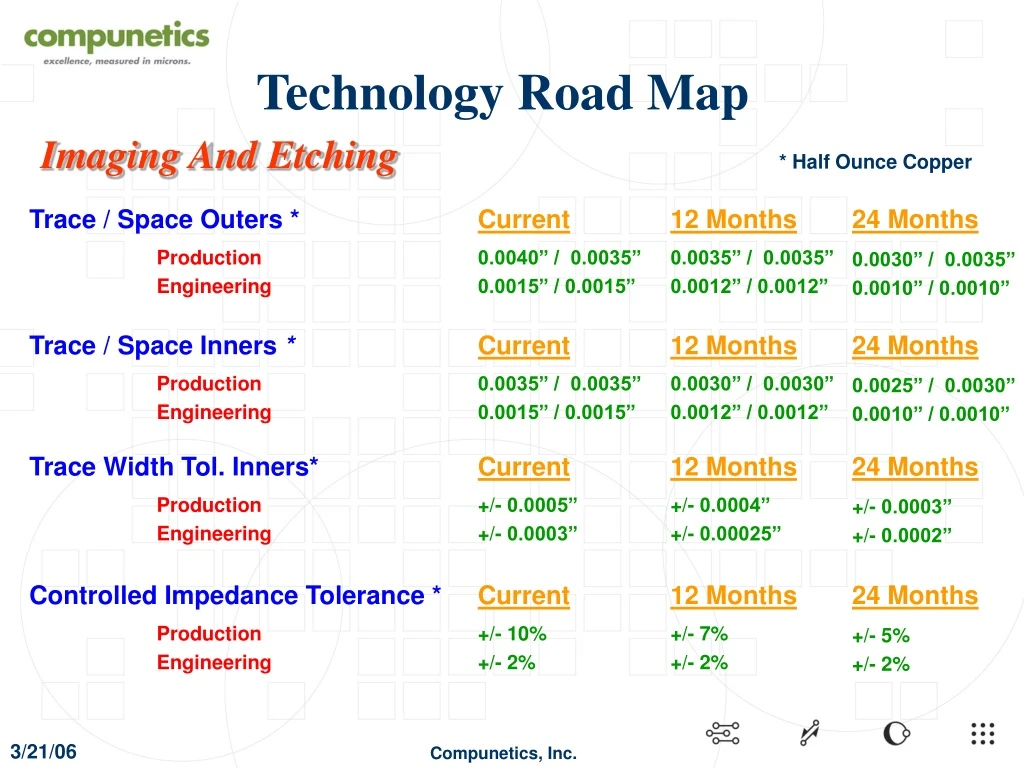
Technology Road Map. Imaging And Etching. * Half Ounce Copper. Trace / Space Outers *. Current. 12 Months. 24 Months. Production Engineering. 0.0040” / 0.0035” 0.0015” / 0.0015”. 0.0035” / 0.0035” 0.0012” / 0.0012”. 0.0030” / 0.0035” 0.0010” / 0.0010”. Trace / Space Inners *.

E N D
Technology Road Map Imaging And Etching * Half Ounce Copper Trace / Space Outers * Current 12 Months 24 Months Production Engineering 0.0040” / 0.0035” 0.0015” / 0.0015” 0.0035” / 0.0035” 0.0012” / 0.0012” 0.0030” / 0.0035” 0.0010” / 0.0010” Trace / Space Inners * Current 12 Months 24 Months Production Engineering 0.0035” / 0.0035” 0.0015” / 0.0015” 0.0030” / 0.0030” 0.0012” / 0.0012” 0.0025” / 0.0030” 0.0010” / 0.0010” Trace Width Tol. Inners* Current 12 Months 24 Months Production Engineering +/- 0.0005” +/- 0.0003” +/- 0.0004” +/- 0.00025” +/- 0.0003” +/- 0.0002” Controlled Impedance Tolerance * Current 12 Months 24 Months Production Engineering +/- 10% +/- 2% +/- 7% +/- 2% +/- 5% +/- 2%
Technology Road Map Imaging And Mechanical Layer-to-Layer Registration Current 12 Months 24 Months Production Engineering +/- 0.0030” +/- 0.0025” +/- 0.0030” +/- 0.0025” +/- 0.0025” +/- 0.0020” Signal Pad Annular Ring Inners Current 12 Months 24 Months Production Engineering 0.0040” 0.0030” 0.0035” 0.0025” 0.0030” 0.0020” Plane Clearance Inners Current 12 Months 24 Months Production Engineering 0.016” 0.011” 0.014” 0.010” 0.012” 0.008” Copper Feature to Board Edge Current 12 Months 24 Months Production Engineering 0.0050” 0.0030” 0.0045” 0.0025” 0.0040” 0.0020”
Technology Road Map Laser Drilled Microvias Minimum Hole to Capture Pad Current 12 Months 24 Months 0.004” / 0.008” 0.002” / 0.005” 0.005” / 0.009” 0.002” / 0.006” Production Engineering 0.006” / 0.010” 0.003” / 0.006” Aspect Ratio of Blind Microvia Current 12 Months 24 Months Production Engineering 0.5:1 0.7:1 0.6:1 0.8:1 0.7:1 1:1 Copper Filled Microvias Current 12 Months 24 Months Production Engineering No Evaluation No Yes Yes Yes Multi-Level Microvias (Stacked) Current 12 Months 24 Months Production Engineering No Yes No Yes Yes Yes
Technology Road Map *.0.062” thick board ** 0.125 thick board Mechanical Number of Layers Current 12 Months 24 Months Production Engineering 26 52 28 56 32 60 Smallest Mechanical Drilled Holes* Current 12 Months 24 Months Production Engineering 0.0060” 0.0040” 0.0060” 0.0040” 0.0050” 0.0030”
Technology Road Map Soldermask And Screening Minimum Soldermask Web Current 12 Months 24 Months Production Engineering 0.0030” 0.0030” 0.0030” 0.0025” 0.0030” 0.0025” Minimum Soldermask Clearance Current 12 Months 24 Months Production Engineering 0.0030” 0.0025” 0.0025” 0.0020” 0.0025” 0.0020” Legend Min Height / Line Width Current 12 Months 24 Months 0.050” / 0.006” 0.040” / 0.005” 0.030” / 0.006” 0.035” / 0.005” 0.035” / 0.005” 0.030” / 0.004” Production Engineering
Technology Road Map Plating Aspect Ratio Current 12 Months 24 Months Production Engineering 9:1 12:1 10:1 13:1 11:1 14:1 PTH Tolerance (finished hole size) Current 12 Months 24 Months Production Engineering +/- 0.0030” +/- 0.0015” +/- 0.0025” +/- 0.0012” +/- 0.0020” +/- 0.0010”
Challenging Technologies Laser Drilled Blind Micro-vias
Extreme Technologies Copper Filled Micro-vias • Via-in-pad Provides Flat Pad Surface for BGA Attach • Flat Surface Optimal For Stacked Micro-vias • Need For Special Plating Chemistry • Need For Special Plating Equipment • Enables Pin Escaping High Pin Count .5 mm Pitch BGAs • Technology Under Development at Several US Shops
Extreme Technologies Copper Filled Micro-vias Current Plating Technology
Extreme Technologies Copper Filled Micro-vias Compunetics Test Results • Test Boards Have Been Received From (2) Chemistry Manufacturers • The Smaller The Hole, The More Flat the Plating • Plating of Close to 1:1 on Blind Microvias • Both Manufacturers to Receive Stacked Microvia Tests • Stress Testing In Progress
Extreme Technologies Copper Filled Micro-vias Stacked Micro-vias
Extreme Technologies Copper Filled Micro-vias Stepped Micro-vias
Extreme Technologies High Aspect Ratio Blind Micro-via Plating • Some Designs Require More Dielectric Between Layers 1-2 and Still Require Blind Micro-vias • Current Technology at approx. 0.7:1 Aspect Ratio • Industry Looking for Aspect Ratios of Greater Than 1.25:1 • Copper Filled Micro-via Chemistry and Equipment May Help Increase Achievable Aspect Ratios
New Equipment Horizontal Plate Through Line • Plate Through Line Designed To Electroless Plate High Aspect Ratio Holes And Blind Laser Drilled Micro Vias • Increased Through Put And Easier Control Of Chemistry • Less Start Up Time For Chemistry