Touch on Nanomaterials
140 likes | 688 Views
Touch on Nanomaterials. Jin Wang Dept. Mechanical and Aerospace Engineering Feb.28,2007. Outline. What is nanomaterial…. Why nano and select methods to fabricate nanomaterials. …. Fabrication of nanocrystals by controlling nucleation and growth process .

Touch on Nanomaterials
E N D
Presentation Transcript
Touch on Nanomaterials Jin Wang Dept. Mechanical and Aerospace Engineering Feb.28,2007
Outline What is nanomaterial… Why nano and select methods to fabricate nanomaterials … Fabrication of nanocrystals by controlling nucleation and growth process Fabrication of nanostructured materials via wet chemical route --Sol-gel --Hydrothermal synthesis Fabrication of nanostructures via top-down lithography strategy
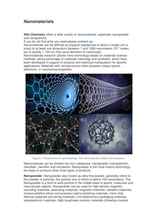
Divide into 1000 equal parts human hair Manmade particles virus ~100nm ~100 mm Artificial nanomaterial 100 nm Natural nanomaterial What is nanomaterials… Generally it refers to the materials whose dimensions (either on 1, 2, or 3 dimensions) are on the order of a billionth of a meter.
http://snf.stanford.edu Intel’s transistors Why nano… Due to the small size… Distinct behaviors while interacting with external stimuli(optic, electric, magnetic…) Promising performance in optical and electrical devices Extraordinarily large surface to volume ratio High-efficiency catalysts, high-sensitivity sensors and transducers Access to better understand the material world on the order which has never been so small ---- to better control the small world
Fabrication of nanocrystals by controlling nucleation and growth process---- fabrication of nanocrystals in glass matrix The formation of crystals always comprise two steps: nucleation-- a process in a phase transition in which nuclei of a new phase are first formed; growth-- the propagation of the new phase at a faster rate. If we provide suitable environment to let the process go on and then cut off to stop the process just after the nucleation or at the early stage of growth, it can be imagined that we can control the size of the as obtained crystals on small scale. Example--fabrication of rear earth doped oxyfluoride glass ceramics Rear earth ions– optical active species Oxyfluoride glass ceramics: Oxide glass matrix– good mechanical properties and stability under harsh environment, widened spectrum band, ability to be fiberized; Fluoride crystals– provide rear earth ions low-phonon environment thus the optical output efficiency is greatly enhanced. Nanocrystals– avoid refraction loss and keep the material transparent in the UV-VIS range ---- key to insure the performance Another bonus: access to investigate the optical properties of rear earth ions in nanocrystals
Fabrication of nanocrystals by controlling nucleation and growth process---- fabrication of nanocrystals in glass matrix • Process: • Melting the raw materials at high temperature (~1400 0C) • rapid quenching to have the oxyfluoride glasses • DTA measurement to find glass transition temperature and crystalization temperature • perform nucleation and growth process under appropriate heat treatment scheme (temperature, time, ramp speed).
Metal alkoxide solution Evaporation Sol Template filling Sol-filled template Evaporation Spin coating Heat Xerogel film Gel Nanotube /Nanowire-filled template Dissolve template Heat Heat Nanograined film Nanoparticles Nanotubes/Nanowires Fabrication of nanostructured materials via wet chemical route -- sol-gel synthesis of La0.6Sr0.4CoO3 nanostructured materials Wet and Chemical: the reaction process which is performed in solution When we want large area-to-volume-ratio of nanomaterials to enhance the efficiency of surface reaction, wet chemical route is a good resort. Mass production and low cost! Example: Our sol-gel process
Fabrication of nanostructured materials via wet chemical route -- sol-gel synthesis of La0.6Sr0.4CoO3 nanostructured materials SEM image of La0.6Sr0.4CoO3 nanograined film AFM image of La0.6Sr0.4CoO3 nanograined film
Fabrication of nanostructured materials via wet chemical route -- sol-gel synthesis of La0.6Sr0.4CoO3 nanostructured materials 500nm SEM image of La0.6Sr0.4CoO3 nanotubes SEM image of La0.6Sr0.4CoO3 nanowires
Fabrication of nanostructured materials via wet chemical route -- Hydrothermal synthesis of nanotubes/nanowires Definition: Techniques of crystallizing substances from high-temperature aqueous solution at high vapor pressure. The term “hydrothermal" is of geologic origin. Tools: The process is performed in an apparatus consisting of a steel pressure vessel called autoclave, in which a nutrient is supplied along with water. How to fabricate 1D nanomaterial: If the product itself has unique preferential crystal structure or, some additives with preferential structure (always organic polymers like PVP, PEG etc) were incorporated into the system, the growth of the new phase will be along one priority crystal direction, thus 1D structure can be obtained.
Fabrication of nanostructured materials via wet chemical route -- Hydrothermal synthesis of nanotubes/nanowires SEM images of hydrogen titanate nanotubes via hydrothermal synthesis at 120ºC SEM images of hydrogen titanate nanowires via hydrothermal synthesis at 200ºC
Fabrication of nanostructures via top-down strategy Crossover with solid state silicon techniques: Utilize lithgraphy (photo lithography, dip-pen, eBeam, SPM…) to generate template; Combined with molecular self-asembly to functionalize template surface. --Provide what experimenter appreciates the most: certainty and controllability Example: Our approach: Combine sol-gel and photo lithography to produce microstructures spin coating photo resist film align mask and UV exposure to do photolithography develop exposed photo resist film and check the template under microscope deposit the material you want (sol-gel spin coating)
Fabrication of nanostructures via top-down strategy The resolution of photo lithography limited the size of structures on the order of micrometers. Ebeam lithography can provide smaller and SPM lithography is able to produce the smallest. The smaller you want, the more difficulties you face. Ebeam lithgraphy and sol-gel S.Donthu, Z.X.Pan, B.Myers, et al, Nano lett. 5, 1710 (2005).
