Download
1 / 44
460 likes | 655 Views
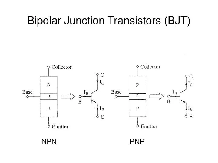
Bipolar Junction Transistors (BJT). NPN. PNP. BJT Cross-Sections. Emitter. Collector. NPN PNP. Common-Emitter NPN Transistor. Reverse bias the CBJ. Forward bias the BEJ. Input Characteristics. Plot I B as f(V BE , V CE )

E N D
BJT Cross-Sections Emitter Collector NPN PNP
Common-Emitter NPN Transistor Reverse bias the CBJ Forward bias the BEJ
Input Characteristics • Plot IB as f(VBE, VCE) • As VCE increases, more VBE required to turn the BE on so that IB>0. • Looks like a pn junction volt-ampere characteristic.
Output Characteristics • Plot IC as f(VCE, IB) • Cutoff region (off) • both BE and BC reverse biased • Active region • BE Forward biased • BC Reverse biased • Saturation region (on) • both BE and BC forward biased
Large-Signal Model of a BJT KCL >> IE = IC + IB βF = hFE = IC/IB IC = βFIB + ICEO IE = IB(1 + βF) + ICEO IE = IB(1 + βF) IE = IC(1 + 1/βF) IE = IC(βF + 1)/βF
DC Load Line VCC/RC VCC
Miller Effect iout vbe vce
Miller Effect (continued) • Miller Capacitance, CMiller = Ccb(1 – A) • since A is usually negative (phase inversion), the Miller capacitance can be much greater than the capacitance Ccb • This capacitance must charge up to the base-emitter forward bias voltage, causing a delay time before any collector current flows.
Saturating a BJT • Normally apply more base current than needed to saturate the transistor • This results in charges being stored in the base region • To calculate the extra charge (saturating charge), determine the emitter current
The Saturating Charge • The saturating charge, Qs storage time constant of the transistor
Switching Times – turn on • Input voltage rises from 0 to V1 • Base current rises to IB1 • Collector current begins to rise after the delay time, td • Collector current rises to steady-state value ICS • This “rise time”, tr allows the Miller capacitance to charge to V1 • turn on time, ton = td + tr
Switching Times – turn off • Input voltage changes from V1 to –V2 • Base current changes to –IB2 • Base current remains at –IB2 until the Miller capacitance discharges to zero, storage time, ts • Base current falls to zero as Miller capacitance charges to –V2, fall time, tf • turn off time, toff = ts + tf
Charge Storage in Saturated BJTs Charge storage in the Base Charge Profile during turn-off
Waveforms for the Transistor Switch VCC = 250 V VBE(sat) = 3 V IB = 8 A VCS(sat) = 2 V ICS = 100 A td = 0.5 µs tr = 1 µs ts = 5 µs tf = 3 µs fs = 10 kHz duty cycle k = 50 % ICEO = 3 mA
Power Loss due to IC for ton = td + tr • During the delay time, 0 ≤t ≤td • Instantaneous Power Loss • Average Power Loss