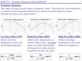
Download
1 / 28
880 likes | 2.2k Views
Frequency Response of Amplifier. Input signal of an amplifier can always be expressed as the sum of sinusoidal signals. The amplifier performance can be characterized by its frequency response. Frequency response of a linear amplifier. Amplifier Transmission or Transfer Function.

E N D
Frequency Response of Amplifier • Input signal of an amplifier can always be expressed as the sum of sinusoidal signals. • The amplifier performance can be characterized by its frequency response.
Frequency response of a linear amplifier Amplifier Transmission or Transfer Function
Amplifier Bandwidth • The figure indicates that the gain is almost constant over a wide range of frequency range ω1 to ω2 . • The band of frequencies over which the gain of the amplifier is within 3dB is called the amplifier bandwidth. • The amplifier is always designed so that its bandwidth coincides with spectrum of the input signal (Distortion less amplification)
Amplifier Transfer Function • Amplifier Types • Direct Coupled or dc amplifier • Capacitively Coupled or ac amplifier • Difference • Gain of the ac amplifier falls off at low frequencies • Amplifier gain is constant over a wide range of frequencies, called Mid-band
Evaluating the Frequency Response of Amplifier • Evaluate the circuit in Frequency Domain by carrying out the circuit analysis in the usual way but with inductance and capacitance represented by their reactances • An inductance L has a reactance or impedance jωL and Capacitance C has a reactance or impedance 1/jωC • The circuit analysis to determine the frequency response can be in complex frequency domain by using complex frequency variable ‘s’ • An inductance L has a reactance or impedance sL and Capacitance C has a reactance or impedance 1/sC
Frequency Response of DC Amplifier Figure 6.12 Frequency response of a direct-coupled (dc) amplifier. Observe that the gain does not fall off at low frequencies, and the midband gain AM extends down to zero frequency.
A resistively loaded MOS differential pair It is assumed that the total impedance between node S and ground is ZSS, consistingof a resistance RSSin parallel with a capacitance CSS. CSS includes Cbd & Cgd of QSas well as Csb1 & Csb2.
Differential Half-circuit. Frequency Response: Differential Gain Frequency Response is the same as studied earlier for common source amplifier.
Figure 6.20 High-frequency equivalent-circuit model of the common-source amplifier. For the common-emitter amplifier, the values of Vsig and Rsig are modified to include the effects of rp and rx; Cgs is replaced by Cp, Vgs by Vp, and Cgdby Cm. Microelectronic Circuits - Fifth Edition Sedra/Smith
Figure 6.23 Analysis of the CS high-frequency equivalent circuit. Microelectronic Circuits - Fifth Edition Sedra/Smith
Figure 6.24 The CS circuit at s5sZ. The output voltage Vo5 0, enabling us to determine sZ from a node equation at D. Microelectronic Circuits - Fifth Edition Sedra/Smith
Quiz # 3 (Syn A) Determine the short circuit transconductance (Gm) of the given circuit.
Quiz # 3 (Syn B) Determine the short circuit transconductance (Gm) of the given circuit.
Common-mode half-circuit. Acm has a zero on the negative real-axis of the s-plan with frequency ωz
Figure 7.37 Variation of (a) common-mode gain, (b) differential gain, and (c) common-mode rejection ratio with frequency.
Figure 7.37 Variation of (a) common-mode gain, (b) differential gain, and (c) common-mode rejection ratio with frequency.
Figure 7.38 The second stage in a differential amplifier is relied on to suppress high-frequency noise injected by the power supply of the first stage, and therefore must maintain a high CMRR at higher frequencies.
Figure 6.22 Application of the open-circuit time-constants method to the CS equivalent circuit of Fig. 6.20. Microelectronic Circuits - Fifth Edition Sedra/Smith
Figure 7.39 (a) Frequency-response analysis of the active-loaded MOS differential amplifier.
Figure 7.39 (a) Frequency-response analysis of the active-loaded MOS differential amplifier.
Figure 7.39 (a) Frequency-response analysis of the active-loaded MOS differential amplifier.
Figure 7.39 (a) Frequency-response analysis of the active-loaded MOS differential amplifier. (b) The overall transconductance Gm as a function of frequency.
Figure 7.39 (a) Frequency-response analysis of the active-loaded MOS differential amplifier. (b) The overall transconductance Gm as a function of frequency.
Figure 7.39 (a) Frequency-response analysis of the active-loaded MOS differential amplifier. (b) The overall transconductance Gm as a function of frequency. The zero frequency (fz) is twice that of the pole (fp2)
Figure 7.39 (a) Frequency-response analysis of the active-loaded MOS differential amplifier. (b) The overall transconductance Gm as a function of frequency.
Assignment # 4 • Carry out detailed frequency response analysis of the current-mirror-loaded MOS differential pair circuit. • Due date: 2 Dec 2011