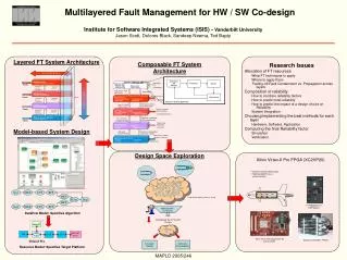
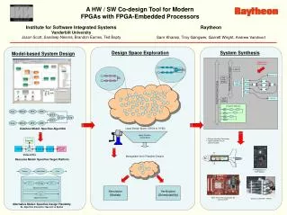
Download
1 / 39
390 likes | 484 Views
Performance evaluation of Virtex-II-Pro embedded solution of Xilinx. Students: Tsimerman Igor Firdman Leonid Supervisors: Rivkin Ina Bergman Alexander. Agenda. Project goals Abstract Project resources System overview System implementation & results

E N D
Performance evaluation of Virtex-II-Pro embedded solution of Xilinx Students: Tsimerman Igor Firdman Leonid Supervisors: Rivkin Ina Bergman Alexander Technion Digital Lab Project
Agenda Project goals Abstract Project resources System overview System implementation & results Results summary Possible improvements Technion Digital Lab Project
Project goals Creation, integration & testing of Xilinx’s PLB Master core using standard IPIF. Comparing between hardware (FPGA) and software (PowerPC based) implementation. Estimation of performance level of Virtex II Pro embedded solution on real digital design example. Technion Digital Lab Project
Power PC 405 Abstract • Some design requires use of external Logic Analyzer for testability purposes. Virtex II Pro may have the capabilities to serve as Programmable On-Chip-Logic Analyzer. • In order to achieve modularity and unification of design, it is preferred to build design around one standard bus. • Power PC or Hardware IP may be served as the analyzing units within Virtex II Pro, therefore their performance must be evaluated for this task on the same standard bus (PLB). Virtex II Pro Test Platform HOST Monitored BUS Technion Digital Lab Project
Project resources Technion Digital Lab Project
Project resources Technion Digital Lab Project
Project resources • Virtex II Pro XC2VP30 – FF896 • ~30K ASIC gates • 136 18x18-bit Multipliers • 2448 Kb of BRAM (18K in each block) • 2 Power PC 405 CPU core (up to 300 MHZ each) • 8 DCM (digital clock manager) units • 8 Rocket IO transceivers (MGTs) Technion Digital Lab Project
PowerPC and Master core doing the same logical function in data analyzing and being compared to each other in the end of the test. Power PC 405 Master core Counter 1 OCM Counter 0 Event counters count random events from Generator (Reference) and Master core. Generator System Overview System block diagram Virtex II Pro Timer (on OPB) Non critical intr Random event SW_EN SW EN block PLB SYS_RST Random event (reference) CLKDV Reset block DCM 0 Generator is creating mass stream of random and sequential data patterns. Technion Digital Lab Project
Power PC 405 2 4 Master core Counter 1 OCM Counter 0 Generator 1 3 System Overview Virtex II Pro Start sequence Timer (on OPB) Non critical intr Random event SW_EN SW EN block PLB SYS_RST Random event (reference) CLKDV Reset block DCM 0 Technion Digital Lab Project
Power PC 405 1 2 Master core Counter 1 Counter 0 OCM Generator System Overview Virtex II Pro Stop sequence Timer (on OPB) Non critical intr Random event SW_EN SW EN block PLB SYS_RST Random event (reference) CLKDV Reset block DCM 0 Technion Digital Lab Project
Power PC 405 Master core PLB System Overview Random Pattern • Random event on PLB = Not increment by one of previous data 344 345 586 587 588 13 14 15 55 55 … Random events Technion Digital Lab Project
Load Count to PLB Counter Din Random delay Max 5 bit Synchronized Random event Load Pseudo-Random Generator Din 32 bit 32 bit Controlled CLK System Overview Generator Block Diagram Technion Digital Lab Project
Pseudo - Random Generator XOR 31 30 3 2 0 1 Shift right each clock System Overview Pseudo-Random Generator • The placement and number of XORs may vary • Random cycle is 2^32 in length • Initial pattern is const Technion Digital Lab Project
System Overview ModelSim simulation results Technion Digital Lab Project
System Overview Chip Scope results Technion Digital Lab Project
System Overview Chip Scope results Technion Digital Lab Project
System Overview Chip Scope results Technion Digital Lab Project
System implementation & Results Power PC • Code and data in OCM • 32 bit data read • Power PC freq. = 300MHz, PLB freq. = 100MHz • The results were displayed at the end of the test via UART (Tera-Pro) Code example: Technion Digital Lab Project
System implementation & Results Power PC – Chip Scope results Note: All Chip Scope results are measured at: PLB sys_clk freq: 100MHz Generator freq: 100/12 (8.33MHz) Technion Digital Lab Project
System implementation & Results Power PC – Chip Scope results Technion Digital Lab Project
System implementation & Results Power PC – Chip Scope results Technion Digital Lab Project
System implementation & Results Power PC – Chip Scope results 20 sys_clocks between PPC read requests. Max freq: ~5MHz Technion Digital Lab Project
System implementation & Results Power PC – Statistics results Technion Digital Lab Project
System implementation & Results Master core • Single transaction configuration • Connected through standard IPIF 2.01a • Performs data analyzing operation similar to PPC operation Code example: Technion Digital Lab Project
System implementation & Results Master core – Chip Scope results Note: All Chip Scope results are measured at: PLB sys_clk freq: 100MHz Generator freq: 100/12 (8.33MHz) Technion Digital Lab Project
System implementation & Results Master core – Chip Scope results Technion Digital Lab Project
System implementation & Results Master core – Chip Scope results 24 sys_clocks between Master core read requests. Max freq: ~4.16MHz Technion Digital Lab Project
System implementation & Results Master core – Statistics results Technion Digital Lab Project
System implementation & Results PPC & Master core – Chip Scope results Technion Digital Lab Project
System implementation & Results PPC & Master core – Chip Scope results PPC: 18-22 sys_clocks between PPC read requests. Aver Max freq: ~5MHz Master:24 sys_clocks between PPC read requests. Max freq: ~4.16MHz Technion Digital Lab Project
System implementation & Results PPC & Master core – Statistics results Note: the statistic results are regarding only PPC transactions Technion Digital Lab Project
ResultsSummary PPC: 20 system clocks between PPC read requests. Max freq: ~5MHz Master: 24 system clocks between Master core read requests. Max freq: ~4.16MHz PPC & Master: PPC:18-22 system clocks between PPC read requests. Aver Max freq: ~5MHz Master: 24 system clocks between PPC read requests. Max freq: ~4.16MHz Technion Digital Lab Project
ResultsSummary Power PC – Alternative test implementation Previous results are valid for certain design. For example, additional statements in PPC design will cause additional delay between PPC read requests and therefore, lower read frequency. Technion Digital Lab Project
ResultsSummary Power PC – Alternative test implementation PPC: 28 sys_clocks between PPC read requests. Max freq: ~3.57MHz Technion Digital Lab Project
ResultsSummary The conclusion: In current configuration Master core throughput is lower than PPC’s. Possible reasons: • PLB protocol limitations in single read transactions (Max freq: sys_clk / 6 = 16.66MHz) • IPIF latency time Technion Digital Lab Project
ResultsSummary PLB protocol limitations Technion Digital Lab Project
ResultsSummary IPIF latency time In this example, master core initiates single read transaction from slave on PLB through IPIF. We can see 23 clocks between Master’s request till valid data on BUS2IP_DATA signals. Technion Digital Lab Project
Possible improvements • PPC: • Code optimization (assembly level) • Avoid single read transactions to the same address whenever possible • Use burst mode and cache transactions. • Master: • Avoid using standard Xilinx IPIF when using Master core on PLB (designing of embedded interface with PLB). • Use FIFO and burst mode transactions. Technion Digital Lab Project
That’s it!!! Technion Digital Lab Project