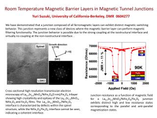
Barrier Layers Technology
Barrier Layers Technology. Prof. Yosi Shacham-Diamand Department of Physical Electronics Tel-Aviv University, Tel-Aviv 69978 ISRAEL. Outline. Introduction Copper Interconnect technology Barrier layers - overview Process development and integration Barrier layers modeling

Barrier Layers Technology
E N D
Presentation Transcript
Barrier Layers Technology Prof. Yosi Shacham-Diamand Department of Physical Electronics Tel-Aviv University, Tel-Aviv 69978 ISRAEL AMC2000
Outline • Introduction • Copper Interconnect technology • Barrier layers - overview • Process development and integration • Barrier layers modeling • Barrier analysis, testing & monitoring • Summary AMC2000
Introduction • Structure of Microchips • ULSI metallization technology • Metallization roadmap • Downscaling issues • Performance issues • Manufacturing issues • Where is the bottom ? AMC2000
Copper multi-level metallization AMC2000
IBM CMOS 7S process AMC2000
Copper chips... • IBM power PC 750 • Mitsubishi Electric eRAMTM family • AMD K7(Athalon) • UMC 0.18 mm process • Motorola 333MHz SRAM • Lucent & Chartered 0.16 mm process AMC2000
IBM PowerPC 750 AMC2000
Interconnect network - 6-7 layers of metallization Silicon substrate (600-800 mm) Active devices layer ( 1-2 mm) Structure of microchips AMC2000
ULSI metallization technology אינטל 2000 AMC2000
Gate and Interconnect delays AMC2000
Delay modeling - the barrier effect • The specific resistance (rb ) of the barrier layers is higher than that of the Cu, (rCu) W H Without barrier: L: line length With barrier (tb: barrier thickness) AMC2000 Assumption: complete barrier coating
Effect of the barrier layer on the interconnect delay Interconnect delay Tint ~ Rint*Cint - including the barrier. In the case of a Damascene technology: For rb >> rCu we get the the interconnect delay increases as the ratio between the actual copper line cross section and the total cross section. AMC2000
Barrier layers - overview Why do we need barriers ? Requirements from barriers AMC2000
Barrier layers for Cu metallization • Why do we need barrier layers? • Copper affects Si properties • Cu affects SiO2 properties • Cu affect most insulators properties • Cu adheres poorly to bottom and side ILD • Why do we need a top barrier (capping layer) • Cu corrodes • Cu adheres poorly to top ILD AMC2000
Requirements from barrier layers • Step coverage on high aspect ratio holes and trenches • Low thin film resistivity • Adhesion to the ILD • Adhesion to Cu • Stable at all process temperatures • Process compatible to the ILD • Process compatible to CMP • Act as a good barrier AMC2000
Barrier layers - types • Sacrificial • Stuffed - impurities in the grain boundaries • Amorphous - no grain boundaries AMC2000
Diffusion barrier - classification of the candidates for barriers that has been investigated in the last 15 years • transition metals • transition metal alloys • transition metal - silicon • transition metal nitrides, oxides, or borides • Miscellaneous: ternary alloys, a-carbon, etc. AMC2000
Summary of barrier layer classification • Transition metals fail as barrier at lower temperatures than their nitrides • transition metal silicides fail due to the reaction of the Si with the Cu. The reaction is most likely to happen at the grain boundaries • Amorphous barriers offer very high reaction temperatures, however, they have very high specific resistivity • The barrier properties depend also on the deposition method. AMC2000
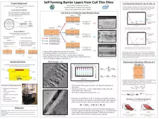
Process development and manufacturing considerations AMC2000
Step coverage issues Barrier layer too thick Barrier layer too thin AMC2000
Coverage issues • Nonuniform sidewall deposition: • agglomeration • Bad coverage at the bottom corner - can be amplified if the bottom corner has some overetch of the layer below AMC2000
The effect of pre-deposition clean on the barrier integrity Physical process in Ar+ ions Reactive clean • Problems • Damage to the barrier • Damage to the dielectric • Barrier metal and Cu • Sputtering and re-deposition on the sidewalls AMC2000
Copper patterning • Dry etch • Difficult, expensive • Conventional equipment • Dual Damascene • Fully planar, lower cost, • New technology AMC2000
Cu process options AMC2000
Electroplating solutions • Cu ions - Cu sulfate • Acid - H2 SO4 for pH adjustment • HCl - Affects Cu surface adsorption; Halide ad-layer drives Cu growth. It also acts as a surfactant and stabilizes grain growth. Cu deposition is driven by the desorption of the halides. AMC2000
Electroplating Based Process Sequence Pre-clean IMP barrier + Copper Electroplating CMP 25 nm 10-20 nm + 100-200 nm Simple, Low-cost, Hybrid, Robust Fill Solution AMC2000
Diffusion barrier for Copper (I) • PVD Ta,TiN, and TaN • Neutrals sputtering • Collimated & Non collimated • Ions sputtering • RF ionized • HCM- Hollow Cathode Magnetron • CVD of TiN • Iodine or Chlorine based chemistry • CVD of Ta and TaN (or both) • Bromide based chemistry • MOCVD of TiN • TDMAT & TDEAT AMC2000
Target Target Target Substrate Substrate Substrate Bias DC magnetron sputtering Collimated sputtering IMP - Ionized Metal Plasma PVD barrier technologies RF AMC2000
Diffusion barrier comparison, (M. Mossavi et al., IITC 98) AMC2000
Vias with IMP TaN AMC2000
Sputtered WxN barrier AMC2000
MOCVD TiN Precursors:Tetrakis-dimethylamino Titanium AMC2000
Other Novel barriers RuO2 r=40-250 mW cm TaSiN,TiSiN r=200-600 mW cm WBN r=300-10000 mW cm CoWP r=20-120 mW cm AMC2000
Electroless barriers Surface activation methods AMC2000
Advantage of Electroless barriers • Conformal • Low cost • Good quality - low r, low stress • can be integrated with electroless copper Barrier Cu ILD AMC2000
Co(W,P) barrier layer AMC2000
Barrier layers modeling • Diffusion models - kinetics • Reaction models - thermodynamics AMC2000
Equilibrium thermodynamics of diffusion barriers (C.E. Ramberg et al., Microelectronics Microengineering, 50 (2000) 357-368) • Cu makes silicides with silicon • Barriers include transition metal+metaloid (Si,B,or N) AMC2000
N TiN Ti2N Cu Cu4Ti Cu4Ti3 CuTi CuTi2 Ternary phase diagrams • The lack of Ta-Cu compounds yield a broad range of compositions in equilibrium with Cu. • Ti-rich compositions are expected to react with Cu N TaN Ta2N Ti Cu Ta AMC2000
Barrier Analysis & monitoring • Materials science techniques: • AES, SIMS, RBS, SEM • Electrical characterization: • I-V • C-V & C-t AMC2000
Electrical characterization: MOS capacitors Capacitance measurements: CV: Flat band voltage, interface states Ct : minority carrier lifetime, surface recombination velocity IV &It: metal/insulator integrity. AMC2000
Ideal MOS capacitance-voltage curve. Solid curve - High f , Dotted curve Low frequencies. Oxide thickness is 140. NA = 1·1015 cm-3. Low frequency High frequency Relaxation High frequency - fast sweep AMC2000