Download
1 / 2
20 likes | 103 Views
This study focuses on semiconductor nanowire growth interfaces, crucial for future electronic devices like transistors and solar cells. By observing nanowire growth in a unique electron microscope, researchers uncover complex catalyst-nanowire structures impacting growth kinetics and crystal structure. Fundamental insights drive the design of new catalyst systems for precise nanowire-based structures, vital for real-world applications. High-resolution images and modeling further elucidate catalyst-nanowire interactions, providing a scientific basis for industrial processes and novel materials development.

E N D
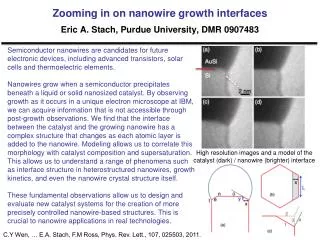
Zooming in on nanowire growth interfacesEric A. Stach, Purdue University, DMR 0907483 Semiconductor nanowires are candidates for future electronic devices, including advanced transistors, solar cells and thermoelectric elements. Nanowires grow when a semiconductor precipitates beneath a liquid or solid nanosized catalyst. By observing growth as it occurs in a unique electron microscope at IBM, we can acquire information that is not accessible through post-growth observations. We find that the interface between the catalyst and the growing nanowire has a complex structure that changes as each atomic layer is added to the nanowire. Modeling allows us to correlate this morphology with catalyst composition and supersaturation. This allows us to understand a range of phenomena such as interface structure in heterostructurednanowires, growth kinetics, and even the nanowire crystal structure itself. These fundamental observations allow us to design and evaluate new catalyst systems for the creation of more precisely controlled nanowire-based structures. This is crucial to nanowire applications in real technologies. High resolution images and a model of the catalyst (dark) / nanowire (brighter) interface C.Y Wen, … E.A. Stach, F.M Ross, Phys. Rev. Lett., 107, 025503, 2011.
Fundamental science that impacts industrial processes Eric A. Stach, Purdue University, DMR 0907483 Atomic resolution electron micrographs of Si / Genanowiremultilayers grown using AuAl alloy catalysts The ability to create these structures is an outgrowth of our fundamental studies During the course of this GOALI project we have systematically investigated the key processes during the creation of nanowire-based structures. We have shown that nanowire nucleation is highly reproducible, and that is possible to control such important aspects of growth as the abruptness of heterointerfaces at the atomic scale. The observations have provided the scientific underpinnings of our understanding of nanowire self-assembly, and help industrial technologists to create new, functional materials systems for applications such as semiconductor electronics and energy conversion. Gold alloy catalyst Silicon nanowire Germanium Silicon Germanium