Download
1 / 26
700 likes | 2.59k Views
Cell#1 教育訓練 by (T3 FAB). Cell#1 Eng. Scott Lan. Chimei Innolux Corp. Nov 10, 2010. 課程簡介. 本課程將介紹 Cell 基本架構及工作原理 Cell#1 製程 & 原理 & 相關 Defect. 講師 : Cell#1 工程部 藍志文 Ext NO:22133. 課程內容. Cell 結構 & 運作原理 Cell#1 Process Flow & Defect PI Coating Line Rubbing Line Assembly line

E N D
Cell#1 教育訓練 by (T3 FAB) Cell#1 Eng. Scott Lan Chimei Innolux Corp. Nov 10, 2010
課程簡介 • 本課程將介紹 • Cell 基本架構及工作原理 • Cell#1 製程 & 原理 & 相關Defect 講師: Cell#1工程部 藍志文 Ext NO:22133
課程內容 • Cell 結構 & 運作原理 • Cell#1 Process Flow & Defect • PI Coating Line • Rubbing Line • Assembly line • Conventions Filling • ODF (One Drop Filling)
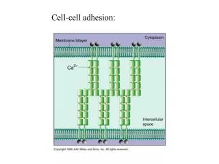
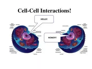
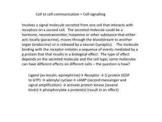
Cell 結構 & 運作原理 • What is TFT LCD? TFT LCD has a sandwich-like structure (Cell or LCD)with liquid crystal filled between two glass plates. TFT Glass has as many transistors as the number of pixels displayed, while a Color Filter Glass has color filter which generates color.
Liquid crystals move according to the difference in voltage between the Color Filter Glass and the TFT Glass. The amount of light supplied by Back Light is determined by the amount of movement of the liquid crystals in such a way as to generate color.
Color Filter - CF 2. TFT - Array • What does Cell#1 have to do? • PI (Polyimide) film coating. – 配向膜成膜. • Rubbing. – 液晶配向. • Assembly. – 對組. • Sealant , AU , Spacer , LC & Aligner • Cell (LCD) structure
Cell (LCD) process flow chart • Cell#1 • Cell#2
PI Coating Line & Process Introduction • PI line profile & process flow chart • PI film特性 • 配向規則力強 • 不含不純物 • 無色,透明性佳 • 高溫,高濕下良好安定性 • 良好的塗佈性與印刷性 • 良好的基板附著性 • 良好的框膠附著性 • 良好的耐熱性
Key process parameter & Defect • Cleaner 使用DI水經超音波輔助,將玻璃上之雜質去除,並經由臭氧(O3)及E-UV將有機物分解.右圖為E-UV工作原理示意圖. 整個流程若潔淨度不佳, 將造成如下圖亮點稱之為 Pin hole.
PI Coater 配向膜(Alignment Layer)其主要的作用為控制液晶分子的排列方向,並提供不同LCD結構所需之預傾角(Pretilt Angle) PI Coating乃採用PI液滾筒塗佈外加APR板之凸板印刷所完成.其中D-Roller & A-Roller之間隙乃為控制PI膜厚度&均勻性之重要參數.
PI Extension Check 每一產品的的開線Setup必須監控PI Extension,過大則會與框膠重疊造成斷線(圖一) ,過小則會造成部份液晶沒有配向產生漏光(圖二). • 圖一 • 圖二
PI Pre Cure & Main Cure PI經過預烤後會經由檢查機檢查印刷品質,其檢驗的重點在於Pin Hole,檢驗完成後即進入約200℃ ~300 ℃烘烤,其所使用的溫度&時間乃依照PI的環化率(Imidization Ratio)來作為參考指標.
PI Rubbing Line & Process Introduction • Rubbing line profile & process flow chart 經過固化之PI膜隨即轉移至Rubbing機台進行配向製程,PI膜經過尼龍(Nylon)或人造絲(Rayon)或天然棉(Cotton)在一定方向進行定向摩擦 (Rubbing) ,產生液晶的配向角(Rubbing Angle)與預傾角(Pretile Angle).
Key process parameter & Defect • Rubbing Station Rubbing製程主要的Key Parameter為 Table Speed , Roller Speed , Cloth Thickness , Motor Torque ( NIP or 壓入量) , 綜合以上參數得以控制良好的Rubbing品質與密度. • Rubbing Density Formula
TN Mode – 垂直配向 • ECB Mode – 平行配向 • Rubbing Defect
Assembly Convention filling line • Convention filling line profile & process flow chart Assembly 主要乃將TFT&CF對準與壓合,但在對準前仍然有幾道製程需各別完成. TFT須灑佈Spacer與AU膠塗佈,CF則須塗佈框膠.
Key process parameter & Defect • Spacer Sprayer Spacer主要用以支撐TFT&CF之間的Cell Gap.一般採用Ball Spacer,其灑佈密度與均勻性為控制的主要項目.如今較先進製程乃採用CF測的 Photo-Spacer. • Spacer聚集 (不均勻) • Photo Spacer示意圖
AU Dispenser 在TFT側特定位置(AU Pad)打上AU seal,當TFT & CF對組壓合後,藉由AU ball傳導,可以將TFT & CF的COMMON點導通.
Sealant Dispenser 在CF側依不同pattern之大小塗佈Seal,經烘烤硬化,以達到TFT & CF對組後之間的黏著力,同時該Seal也是液晶的邊界. • Panel示意圖 • Bi-pane示意圖 • Gap Former 利用上下定盤的高溫及高壓,將基板壓合至所需要的cell gap
Assembly ODF line • ODF line profile & process flow chart ODF line基本上與Convention filling line大同小異,主要乃將TFT&CF對準與壓合,但在原傳統線上的製程增加LC Dispenser, Gap Former也由一真空對組的Chamber取代,以及UV曝光機.
LC Dispenser LC Dispenser在於ODF製程裡頭扮演一個相當重要的腳色,LC藉由一個能夠精準控制LC滴下重量及滴下位置的機構將LC在CF & TFT尚未貼合前就已經滴入. • LC Dispenser示意圖 • Niagara SSH & LC Qty. • Bubble Issue
LC Multi-Dosage LC Multi-Dosage主要是應CF SS均勻性不佳所產生,當分佈於大板上的各Panel SS有所不同時,則各Panel所應注入的LC亦有所不同. 1. SSH 量側 2D Map 2. Panel SSH 量側值 3. 確認Panel LC QTY.
P P P P P CF substrate PS1 PS2 PS2 PS2 PS2 δh ΔH PLN TFT substrate P P P P P • LC Qty. Window 1 atm. (1 大氣壓) ODF Margin δ h ≦ Δ H ODF Margin = δ h / PS Height (Target) = δ h / Cell gap (Target, Tm) δ h to be defined by Shimadzu Data (deformation v.s. force) 1 atm. δ h : Max. Compressible Deformation for PS1 (PS) Δ H : Hybrid delta Height (PS1, PS2) δ h ≦ Δ H ; Δ H ≒ 0.5um @ 1000 ms exposure time for PLN Mask
Cell Gap (um) ← ODF Margin → Mura Margin #B Margin #A CM C0 Margin for ODF by LOT Mura inspection spec. (Cell gap>=PS Height) CB Margin for ODF by PS compressible deformation (max.) Bubble LC Amount (mg or %) L0 LM LB • ODF Margin Definition C0 = PS Height (Target) • Total ODF margin = Margin #A + Margin #B • = LB to LM = CB to CM • 2. Margin #A =δ h (Max.) = C0-CB • = Max. Compressible Deformation for PS1 • it will be the real ODF margin for ODF Bubble • Margin #B = L0 ~LM • ( window gained by Mura inspection spec.)
VAS Chamber VAS chamber主要是將CF & TFT於一真空環境下將其對準貼合,假若貼合真空度不足則會產生氣泡. • Out Gassing Bubble