Electronic Energy Levels Alignment of Dye Sensitized Oxide Surfaces
Electronic Energy Levels Alignment of Dye Sensitized Oxide Surfaces. Sylvie Rangan Rutgers University Department of Physics and Astronomy 136 Frelinghuysen Road, Piscataway, NJ 08854. Introduction. A Dye Sensitized Solar Cells (DSSCs): a potential low cost alternative

Electronic Energy Levels Alignment of Dye Sensitized Oxide Surfaces
E N D
Presentation Transcript
Electronic Energy Levels Alignment of Dye Sensitized Oxide Surfaces Sylvie Rangan Rutgers University Department of Physics and Astronomy 136 Frelinghuysen Road, Piscataway, NJ 08854
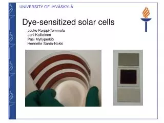
Introduction A Dye Sensitized Solar Cells (DSSCs): a potential low cost alternative to Si solar cells. -Sunlight enters the structure, excites electron-hole pairs in dye. -Electron is transferred into TiO2 conduction band, and hole is filled by I- ions (3I- 2e- + I3-). -Electron travels through circuit, reduces I3- (2e- + I3- 3I-)
e- hn e- TiO2 Energetics: N3 molecule on TiO2 Calculated Structural and Electronic Interactions of the Ruthenium Dye N3 with a Titanium Dioxide Nanocrystal, Petter Persson and Maria J. Lundqvist, J. Phys. Chem. B 2005, 109, 11918-11924 50 fs LUMO I-/I3- HOMO Electrolyte N3
New experimental approach of the subject A few examples to show you it works!
UV Inverse Photoemission Ultra-violet Photoemission LUMO + 1 LUMO + 1 LUMO LUMO HOMO HOMO Experimental setup Occupied and unoccupied states in the same UHV system
Experimental setup Scanning Tunnel Microscope I VT-SPM OMICRON
Outline N3 adsorption Single crystals ZnO(11-20) TiO2(110) rutile Technologically relevant substrates TiO2 anatase nanoparticules ZnO nanorods Direct information electronic structure analogue to N3 linker to the substrate Comparison N3 - INA
Outline ZnTPP derivatives Band alignment determination Single crystals ZnO(11-20) TiO2(110) rutile Band alignment tuning strategies
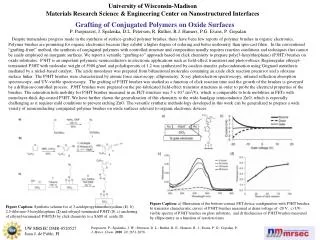
80 nm x 80 nm TiO2 (110) monocrystal Sensitization in acetonitrile solution UHV surface passivation with pivalate ions (CH3)3CCOO- UHV surface preparation Atomically resolved TiO2(110) TiO2(110) Pivalate layer N3/TiO2 30 nm x 30 nm 30 nm x 30 nm
TiO2 (110) IPS UPS 3.4 0.2 O2p Ti3d TiO2(110)
3.6 eV Energydiagram LUMO + 1 LUMO 0.5 eV 3.2 eV Ti3d HOMO LUMO 0.9 eV TiO2(110) HOMO N3 + TiO2(110) N3 TiO2
Influence of intermediate steps HOMO and LUMO due to N3
(0.5 eV) (3.2 eV) (0.9 eV) TiO2 conducting glass Anatase TiO2 nanoparticles LUMO + 1 LUMO 0.7 eV Ti3d 3.1 eV 3.8 eV TiO2 nano N3 + TiO2 nano HOMO 1.5 eV Dunbar P. Birnie III group, Rutgers University • Same HOMO-LUMO gap • Anatase gap 0.2 eV larger • than rutile gap N3 TiO2 100 Å (N3 on TiO2(110))
Comparison with DSSC perfomances Incident Photon to Current conversion Efficiency UPS-IPS LUMO 0.2 eV Ec=0.6 eV 1.5 eV Ef=0 -0.9 eV N3+nanocrystals TiO2 HOMO From Photoelectrochemical cells, Michael Grätzel, Nature, nov 2001, 338 Ev=-3.2 eV Minimum photon energy that produces current: 1.6 eV TiO2 nanoparticles N3
ZnO substrates Monoatomic step edge ~ 2 Å 100 nm x 100 nm Length (nm) ZnO (11-20) epitaxial film • ZnO nanorods: • Grown by Metalorganic • chemical vapor deposition • Length: 1.8 µm • Diameter: 100 nm Yicheng Lu group, Rutgers University
N3 on ZnO(11-20) LUMO + 1 LUMO 2.1 eV 0.4 eV 3.2 0.4 4.5 eV Zn3d O2p Zn4sp 3.2 eV HOMO 1.3 eV • ZnO Gap: 3.6 eV • ZnO Gap: 3.6 eV • Dyefeaturesclearlyvisible N3 ZnO
N3 on ZnO - nanorod LUMO + 1 LUMO 2.0 eV 2.7 eV (2.1 eV) 0.4 eV (0.4 eV) 4.5 eV Zn3d O2p (4.6 eV) 3.4 eV (3.2 eV) HOMO 1.3 eV (1.3 eV) • Smallerdyecoverage • Similar to single crystalZnO N3 ZnO
Isonicotinic acid : N3 linker analogue • INA analog to the N3 Dye linker • In a simple model, compared to N3, • the INA electronic structure should have: • No Ru-N=C=S like HOMO • A LUMO of similar character as • the N3 LUMO
N3-INA comparison TiO2 ZnO INA TiO2 ZnO N3
INA on TiO2 model calculations (1) (2) (1) DFT Study of Bare and Dye-Sensitized TiO2 Clusters and Nanocrystals; Lundqvist, Nilsing, Persson, Lunell Intern. Journal of Quantum Chemistry, Vol 106, 3214–3234 (2006) (2) Anchor group influence on molecule–metal oxide Interfaces: Periodic hybrid DFT study of pyridine bound to TiO2 via carboxylic and phosphonic acid; M. Nilsing , P. Persson, L. Ojama Chemical Physics Letters 415 (2005) 375–380
First Conclusion • UPS and IPS in the same UHV system: • The most direct method to characterize the ground state electronic structure • UV-visible absorption(exciton)/NEXAFS(core hole) typically used in the field • First measurement of the electronic occupied/unoccupied structure of dye molecules on surfaces • Can help improve theoretical treatment of dye/oxides systems. • Energy level alignment of N3 on TiO2(110) and ZnO(11-20) • N3 on TiO2nanoparticles and ZnOnanorods • INA vs N3: linker group good model for LUMO
Zn-TetraPhenylPorphyrin • Appropriate HOMO/LUMO levels position in energy. • Functional groups added to the phenyl groups have not much influence on the TPP absorption properties. ZnTPP Zinc TetraPhenylPorphyrin
ZnTPP vs ZnP HOMOs LUMOs
e- hn e- TiO2 Energy levels alignment E. Galoppini, Rutgers LUMO HOMO Electrolyte ZnTPP
Approaches for band alignment tuning Adding a built-in dipole Effect on electron transfer? Molecule/Molecule interaction Adding spacer between them Changing the linker to the surface
Approaches for band alignment tuning Modifying the ring electronic properties Ex: Electron withdrawing groups Fluorination
ZnTPP1 on TiO2 IPS UPS ZnTPP1+TiO2 ZnTPP1 ZnTPP1 TiO2(110) TiO2(110)
3.6 eV Energy level alignment LUMO + 1 LUMO 2.1 eV 40.8 eV HOMO 2.6 eV ZnTPP1 TiO2 Electronic structure and molecular orientation of a Zn-tetra-phenyl porphyrin multilayer on Si(111) C. Castellarin Cudia et al. 90 eV
Comparison with other methods 1/2 LUMO + 1 LUMO 2.1 eV 0.5 eV 3.5 eV 3.2 eV HOMO 2.6 eV 0.9 eV ZnTPP1 N3 Electron Injection and Recombination in Dye Sensitized Nanocrystalline Titanium Dioxide Films: A Comparison of Ruthenium Bipyridyl and Porphyrin Sensitizer Dyes Yasuhiro Tachibana, Saif A. Haque, Ian P. Mercer, James R. Durrant and David R. Klug, J. Phys. Chem. B, Vol. 104, No. 6, 2000 TiO2
Comparison with other methods 2/2 UPS-IPS LUMO 2.0 eV Ec=0.6 eV Ef=0 HOMO Ev=-3.2 eV 650–700 nm ZnTPP TiO2(110) TetrachelatePorphyrinChromophores for Metal Oxide Semiconductor Sensitization: Effect of the Spacer Length and Anchoring Group Position Jonathan Rochford, Dorothy Chu, Anders Hagfeldt, and Elena Galoppini JACS 129 (2007) 4655
ZnTPP1 electronic structure Phenyls Simple model for simulated DOS DOS = overlap ZnP + Phenyls groups Phenyls Two part electronic structure for the free molecule ZnP HOMO+LUMO: fixed energy Phenyls: position depends on electron withdrawing groups Photoemission cross-section not included ZnP HOMOs ZnP LUMOs
Tunnel Microscopy Approach Sensitization in ethanol solution UHV surface passivation with pivalate ions (CH3)3CCOO- UHV surface preparation Atomically resolved TiO2(110) TiO2(110) Pivalate layer ? 6 Å 3 nm x 2 nm 80 nm x 80 nm 30 nm x 30 nm 30 nm x 30 nm
ZnTPP3 adsorption 20 Å Diameter ̴ 20 Å 100 nm x 100 nm Pivalic acid layer 30nmx30nm Effect on the electronic structure Adsorption modes? Aggregation?
Another conclusion ZnTPP derivatives good candidate to study fundamental properties related to energy level alignment…. …UPS/IPS useful and direct way for measuring energy level alignment…. …Still a lot of work to do!
THANKS !!! Ryan Thorpe Jean-Patrick Theisen Eric Bersch Robert A. Bartynski Senia Katalinic
Absorption properties Typical UV-visible absorption spectrum Soret (or B band) at 400 nm S0 S2 transition Weaker Q band at 550 nm S0 S1 transition • S1 and S2 first and second excited states of the molecule. • Fast internal conversion S2→ S1 • B and Q bands both arise from p to p* transitions and can be explained by considering the four frontier orbitals of the porphyrin.
Goutermann Four-Orbital Model Orbitals LUMOs HOMOs Energy states Soret (B) band S2 Q bands S1 • Transitions between these orbitals gives rise to two 1Eu excited states. • Orbital mixing splits these two states into a high energy state with a high oscillator strength and a low energy state with a low oscillator strength. S0
Pivalic acid covered surface 6 Å 3 nm x 2 nm 15 nm x 15 nm
Zn-based dyes ZnTPP2 ZnTPP1 These dye are believed to adsorb perpendicular to the substrate and might form clusters of parallel molecules.
Zn-based dyes ZnTPP3 This dye is believed to adsorb flat on the substrate.
ZnTPP1 on TiO2 and ZnO Small effect on ZnTPPelecronic structure by changing the substrate.
Approaches for band alignment tuning 3/3… Modifying the ring electronic properties Metal ion

