Download
1 / 12
120 likes | 157 Views
Learn the basics of PCB design with this comprehensive guide covering traces, pads, and component labeling. Explore top and bottom trace views and understand the layout of board and pad groups.

E N D
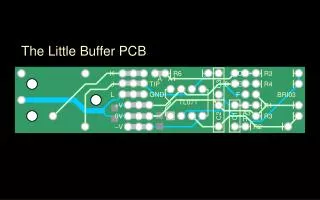
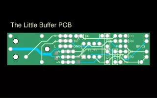
The Little Buffer PCB K R6 C3 C R3 A A1 TIP R4 J D E GND L F BRI03 TL071 +V C2 C1 R1 A3 0V R3 H –V R2
K C3 C R3 A A1 TIP R4 J E GND L F BRI03 TL071 +V C2 C1 R1 A3 0V R3 H –V R2 R6
K C3 C R3 A A1 TIP R4 J E GND L F BRI03 TL071 +V C2 C1 R1 A3 0V R3 H –V R2 R6
K C3 C R3 A A1 TIP R4 J E GND L F BRI03 TL071 +V C2 C1 R1 A3 0V R3 H –V R2 Its Labeling R6 D
K R6 C3 C R3 A A1 TIP R4 J D E GND L F BRI03 TL071 +V C2 C1 R1 A3 0V R3 H –V R2 The top traces
K R6 C3 C R3 A A1 TIP R4 J D E GND L F BRI03 TL071 +V C2 C1 R1 A3 0V R3 H –V R2 The bottom traces (viewed from the top – as if the PCB was transparent)
K R6 C3 C R3 A A1 TIP R4 J D E GND L F BRI03 TL071 +V C2 C1 R1 A3 0V R3 H –V R2 LABELING GROUP
K R6 C3 C R3 A A1 TIP R4 J E GND L F BRI03 TL071 +V C2 C1 R1 A3 0V R3 H –V R2