Download
1 / 34
340 likes | 524 Views
Controlling the thickness of CuCl thin films and improving their quality by means of MBE method. Ashida lab. M1 K amizono Kenta. Contents. Introduction All-optical switching devices Excitons and light in the high-quality system Background Previous results

E N D
Controlling the thickness of CuCl thin films and improving their quality by means of MBE method Ashidalab. M1 Kamizono Kenta
Contents • Introduction • All-optical switching devices • Excitons and light in the high-quality system • Background • Previous results • Temperature dependence of DFWM spectrum • Purpose • Experimental results • Summary DFWM(Degenerated Four Wave Mixing):縮退四光波混合
Introduction All-optical switching devices 光スイッチ Realization by nonlinear optical effect 非線形光学効果 All-optical switching devices • all-optical information processing • superior performances than electronic communication devices • transmission rate伝送効率 • energy efficiency エネルギー効率 Optical switching device Transient grating 過渡回折格子 Probe pulse Signals Pump pulses
Introduction Low consumption energy 低消費エネルギー resonance between light and excitons High response speed高速応答 nonresonance between light and excitons Exciton and trade-off problem + Exciton Trade-offproblem - • high efficient response 高効率応答 • available in the micro crystal Means of confining excitons in the micro crystal can break down this problem.
Introduction Spatial interplay between waves of excitons and light Ref: T. Itoh, M. Furumiya, and T. Ikehara, Solid State Commun. 73, 271 (1990). Nanostructure Long wavelength approximation (LWA) regime 長波長近似領域 Light • size << wavelength of light • dominant interplay between the exciton of lowest state and light • Oscillator strength increaseswith the system size. Dependence of the exciton radiative decay time in CuCl microcrystals n = 4 n= 3 over LWA n= 2 n= 1 Exciton
Introduction Excitons and light in the high-quality system System where exciton wave functions are coherently extended to the whole volume Light Nanostructure LWA regime Light • Coupling of multinode-type excitons with light • The coupling with the size increase is not limited. n = 4 n= 3 Exciton n= 2 Ultrafast response beyond LWA regime n= 1 Exciton
Introduction Radiative corrections (輻射補正) in the coupled system of photons and excitons Ref: H. Ishihara, J. Kishimoto and K. Sugihara, J. Lumin. 108, 343 (2004). Size dependence of radiative corrections for the CuCl Z3 exciton (theory) 330nm Imaginary part of radiative corrections Real part of radiative corrections Uncoupled excitonic modes Radiative width:Γn Eigenenergy including the radiative shift τ :radiative decay time τ= ħ/2Γn
Background Property of CuCl direct transition semiconductor E Z3 Z1,2 Cu+ Cl- • large exciton binding energy (200 meV) • small exciton Boar radiance (0.7 nm) • The center-of-mass confined effect of excitons is available. Suitable material for research of the center-of-mass confined effect of excitons k Zinc Blend
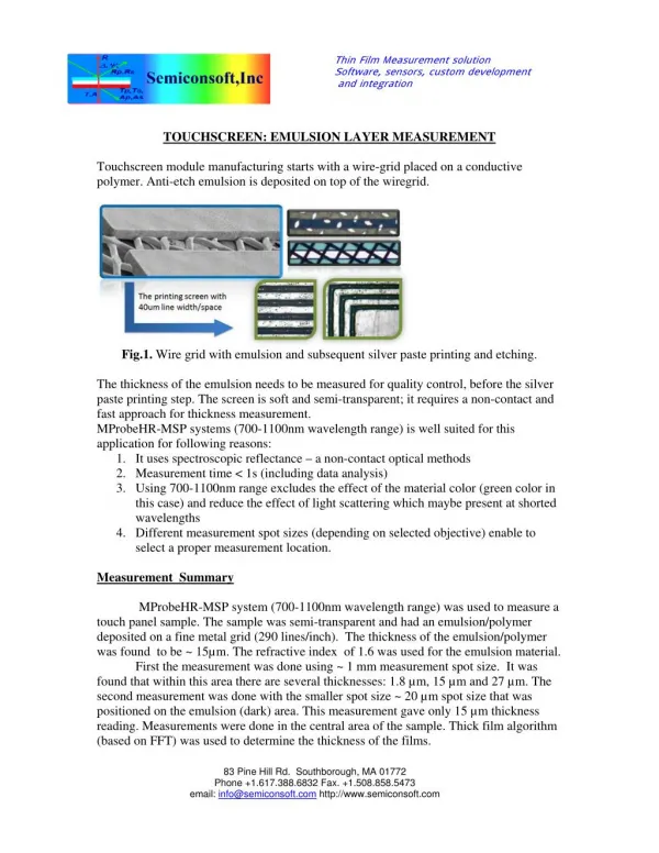
Background Growth of high-quality CuCl thin films Atomic Force Microscope; AFM AFM image of CuCl thin film AFM image of high-quality CuCl thin film (by RHEED) 40nm CaF2cap layer e-beam-exposed CuCl layer Surface morphology is extremely improved by electron beam irradiation. CaF2buffer layer 40nm 1mm CaF2(111) substrate
Previous results Mode structures of DFWM spectrum in a high-quality CuCl thin film • Several peak structures appear. • Good agreement with eigenenergy including the radiative shift M. Ichimiya, M. Ashida, H. Yasuda, H. Ishihara, and T. Itoh, Phys. Rev. Lett. 103, 257401 (2009) 261nm Degenerated Four Wave Mixing(DFWM) 2k2ーk1 k1 k2 2k1ー k2 Eigenenergy including the radiative shift Radiative width
Previous results Temperature dependence of DFWM spectrum (68 nm) Calculated induced polarization spectra Radiative width(meV) DFWM spectra n = 1 n = 2 n = 3 1.8 5.0 0.29 • Both spectral dependences are same. • A component for n=2 becomes dominant as the temperature increases. The excitonic state with the largest radiative width may be observed at high temperatures.
Previous results Temperature dependence of DFWM spectrum (310 nm) M. Ichimiya, K. Mochizuki, M. Ashida, H Yasuda, H. Ishihara, and T. Itoh, Phys. Status Solidi B 248, 456–459 (2011) • Spectral shape changes as temperature increases. • Components with smaller radiative width disappear at lower temperatures. • A component for n = 5 becomes dominant and only the state is observed above 210 K. Radiative width(meV) n = 6 n = 8 n = 5 n = 7 19 1.4 0.27 0.46 DFWM signal can be observed at room temperature!
Purpose Light Light Exciton • Deciding the condition of fabricating CuCl thin film by means of molecular beam epitaxy (MBE) method (329nm) • Fabricating high-quality CuCl thin film on improving the quality High-quality Exciton • Realizing ultrafast radiative decay by the curtain thickness on large radiative width • Enhancement of DFWM signal on improving the quality of CuCl thin film Realization of efficient and ultrafast radiative decay above room temperature
Experimental Procedure RHEED Molecular Beam Epitaxy(MBE) method pump melting pot 329 nm substrate screen shutter CuCl layer substrate temperature : 50~150 0C growth rate: 0.13 nm/s oscillator crystal shutter CuCllayer CaF2buffer layer substrate temperature :600 0C growth rate : 0.02 nm/s CaF2buffer lay K-cell 40nm CaF2 CuCl CaF2(111) substrate 1mm Vacuum 1.0×10⁻⁶~ 9.0×10⁻⁷ Pa
results Transmission of normal incident light in the transparent region (150 ℃) L n= 2 n = 1 Light • The difference is not same. CuCl evaporate on the substrate again. Lower substrate temperature
results Transmission of normal incident light in the transparent region (130 ℃) L n= 2 n = 1 Light The differences are same at lower substrate temperature. What quality does the CuCl thin film have
results AFM image (150℃) ’11 01/13 ’10 12/23 20 nm 20 nm 3 μm 3 μm Surface morphology is extremely-good.
results AFM image (under 130℃) ’11 02/20 ’11 02/24 20 nm 20 nm 3 μm 3 μm Surface morphology is extremely-good. Which is better, high substrate temperature or low?
Experimental configuration Degenerated Four Wave Mixing (DFWM) spectroscopy SHG crystal BS Mode-locked Ti:sapphire laser Pulse width:110 fs Repetition:80 MHz wavelength:387nm CCD Monochro- mator Cryostat(6K) Optical fiber Sample(CuCl)
results DFWM spectrum in high-quality CuCl thin film (150℃) Thickness 313nm 6K • Photon energy of each peak is in goodagreement. • Sharp peak structures appear. 313nm High-quality CuCl thin film
results DFWM spectrum in high-quality CuCl thin film(50℃) Thickness 235nm 6K • DFWM spectrum depends on the thickness of CuCl thin film. • Photon energy of some peak is in good agreement • Peak structures with small radiative width don’t appear • This CuCl thin film is not so high-quality 235nm High substrate temperature is important.
Summary • The difference between the crystal oscillator and measured thickness is not same (150℃), but it is same (130℃). • Surface morphologies (150 and 130℃)are extremely-good. • Sharp peak structures appear (150℃). • DFWM spectrum depends on the thickness of CuCl thin film. Evaporation on the substrate of CuCl thin film Surface morphology DFWM spectrum
Previous results Radiative width and decay time (310 and 329nm) Film thickness dependence of calculated radiative width n=5 exciton maintains high efficient radiative decay beyond nonradiative decay. Optimizing the thickness of CuCl thin film will realize ultrafast radiative response than 10 fs. Film thickness dependence of calculated radiative decay time
Reflection High Energy Electron Diffraction (RHEED) e-beam substrate CaF2cap layer 40nm CuCllayer e-beam-exposed CaF2buffer layer 40nm CaF2(111) substrate 1mm
Background Ga GaAs As F defection E-beam exposed Growth of high-quality CuCl thin films by e-beam exposed H. C. Lee et al. Japan J. Appl. Phys. 26. 11. pp. L1834-L1836. 1987 CaF2 F
Background 縮退四光波混合(DFWM) 過渡回折格子 プローブ光 DFWM信号 ポンプ光 2本のポンプ光が入射して、過渡回折格子が生成される。 過渡回折格子によって、プローブ光が回折される。 信号光が観測される。 2本ポンプ光とプローブ光の時間差が0 非線形光学強度 ポンプ光間の時間差が0 過渡回折格子の緩和
CuCl CaF2 Fluorite Zinc Blend Cu+ Ca2+ Cl- F-
Future prospect • Fabricating the CuCl thin film (320~340nm, 130℃) • To keep high-quality of sample, fabricating cap layer • Measuring the quality of CuCl thin film by DFWM spectroscopy • Saving CuCl thin film from degradation • Repeating experiments DFWM spectrum in a CuCl thin film having cap layer (<10K) 329nm CuCl layer 40nm CaF2cap layer CaF2buffer layer 40nm CaF2(111)substrate 1mm Advantage of cap layer First After Leaving it out in the air for 30 hours
results Transmission ’10 12/15 ’10 11/18
results AFM image ‘10 11/11 ‘10 11/18 40 nm 20 nm 3 μm 3 μm ‘10 12/15 20 nm 3 μm
results Transmission 10,11/30 10,12/02
results AFM image 20 nm 3 μm ‘10 12/02 ‘10 12/02