Chapter 5 Microprocessor Caches
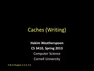
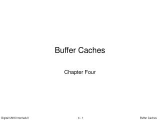
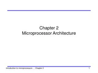
Chapter 5 Microprocessor Caches. Levels of the Memory Hierarchy. Capacity Access Time Cost. Upper Level. Staging Transfer Unit. faster. CPU Registers 100 Bytes <10s ns. Registers. prog./compiler 1-8 bytes. Instr. Operands. Cache K Bytes 10-100 ns. Cache. cache control

Chapter 5 Microprocessor Caches
E N D
Presentation Transcript
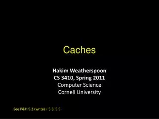
Levels of the Memory Hierarchy Capacity Access Time Cost Upper Level Staging Transfer Unit faster CPU Registers 100 Bytes <10s ns Registers prog./compiler 1-8 bytes Instr. Operands Cache K Bytes 10-100 ns Cache cache control 8-128 bytes Blocks Main Memory M Bytes 100ns-1us Memory OS 512-4K bytes Pages Disk G Bytes ms Disk user/operator Mbytes Files Larger Tape infinite sec-min Lower Level Tape
5.1 Introduction • Memory speed : SRAM > DRAM > second memory (hard disk) • Cache hit: requested instruction/data by microprocessor is found in the cache • Cache miss: request instruction/data is not in the cache => read from main memory (DRAM) and the associated data is copied in the cache (cache update)
Cache improve overall system performance by: • Improve read cycle • Improve write cycle • Reducing the traffic on the memory bus (system bus) (other bus master or microprocessor can use the system bus) • Cache memories work on the principles of • Spatial localities: the processor is likely in the near future to need the information it is working on at the present • Temporal localities : programs tend to use recent information
Cache performance is measured by its hit rate: cache hit rate (or hit rate) • hit rate % = cache hits/(total memory requests) * 100% • miss rate = 1- hit rate • cache miss penalty: time it takes to access main memory, fetch a block, update an entry in the cache, and send the requested item to the microprocessor • processor stall: the microprocessor must wait for the memory system re respond • In gerneral, Average Access Time: • = Hit Time x (1 - Miss Rate) + Miss Penalty x Miss Rate
5.2 System Issues • external caches (level 2 cache) and internal caches (level 1 cache) (multilevel caches) • Real (physical) cache : caches receive physical addresses, usually from an MMU that has already done the virtual-to-physical address conversion • Virtual (logical) cache: cache receive unconverted virtual addresses
There are two alternative to placing the cache between the microprocessor and main memory • look-through architecture (serial cache read architecture): first access the cache, if miss, then access main memory => long microprocessor stall. Fig. 5.3 • look-aside architecture (parallel cache read architecture): microprocessor starts cache and main memory accesses simultaneously. Fig. 5.5 => memory subsystem are kept busy
Write policies • write through • 任何時間, 若cache內之資料有被修改, 則亦立即修改主力體內之相對內容寫的次數將很多 • buffer write-through: use write buffers to decouple the write operations of the CPU from external bus writing to main memory Fig. 5.7 • write back • 當cpu要須改cache內容時, 僅修改cache • 僅當此slot要被換掉時, 才其內容寫到主記憶體內 • 會有cache coherency 的問題, 即cache內的內容會和主記憶體的內容不同 Cache Processor DRAM Write Buffer
Cache 和主記憶體間的介面 • Cache分成C個line (or block), 每個line內有2W個word, 每個word有2B bytes • Cache是以每次2W words 的長度由主記憶體搬到cache (line fill) • 若主記憶體內有有n條位址線(X+W+B), 則有可分成2X= 2n/ 2W+B blocks, 2X >> C • 到底主記憶體的那個block被放到cache內的那個line,是靠tags來判斷 • 若cache內之一個slot要被換掉時, 我們必須將此slot內有被更改過的內容寫回主記憶體
主記憶體和cache間的對應方式 • 因為 M>>C,所以才有mapping的問題 • 直接對應(direct mapping) • 關聯式對應(fully associative mapping) • 集合式關聯式對應(set associative mapping)
5.3.1 Fully Associative • Fig. 5.10, each cache line has 4-word, each word has 2-byte, the cache has 8 lines, the main memory has 128-byte
Full associative • The advantages and disadvantages • Most expensive and complexity: the number of comparators equal to the number of lines in the cache • Lower cache miss probability • Doesn’t has thrash • Require replacement algorithm: LRU (least recently used)
Ex: 5.1 If main memory is 16 Mbytes, and is considered subdivided into blocks of 4 bytes each, then a fully associative cache line will have a 4-byte block and a 22-bit cache tag.
5.3.2 Direct Mapped (C sets, K=1 way) • 64 bytes cache, each line has 4 words (8 bytes) • Block d of main memory will be placed in the block f of cache, where f = d mod c EX 5.2
Direct mapped • Only one comparator • Has a thrashing problem • Don’t need replacement algorithm • higher cache miss probability
5.3.3 Set-Associative • K-way set-associative • Each set has K-line, the number of sets is S=C/K
5.3.4 General Cache Structure • Three different K-way set-associative cache memory organization • Fully associative (K=C, S=1) • Direct mapped (K=1, S=C) • K-way set-associative (S=C/K)
5.3.5 Cache line status bits • Line valid bit: valid cache line • Invalid tag means: the corresponding block in main memory has been modified by another bus master, and the data in the cache has not been updated (cache line data is stale) • Word valid bits: • Instead tag valid bit, provide separate valid bits for 32-bit or 16-bit word • Word dirty/modified bits • When the processor has updated the word in the cache. The main memory contain the stale data • LRU field: for least recently used replacement algorithm • Exclusive ownership bits: • To indicate whether the data is exclusive to the cache or resides in other caches of the system • Access-rights and process-ID fields • Parity bits
5.4.3 Cache line fill techniques • Multiple bus cycles • For 80486, 16 bytes nonburst line fill: 2-2-2-2, for burst line fill: 2-1-1-1 • Data requested last: • The data item requested is placed in the cache last • Ex: for 32-bit CPU with 16-byte cache line requesting a data item from location 16N+4 of a 32-bit memory 16N+8, 16N+C, 16N, 16N+4 • Has a high miss penalty
Data request first • The line fill first fetches the requested data item and simultaneously passes it to the microprocessor 16N+4, 16N, 16N+C, 16N+8
Line buffer caching • When the microprocessor requests data, both the cache data RAM and the line buffer are checked to see if the information is valid
5.5.2 direct Mapped : Motorola 68030 • it is a RISC CPU with Harvard architecture (CISC is von Neumann architecture), split-cache on-chip cache (instruction cache and data cache), virtual cache, it contains 256 byte ( 16 line (slot), each line has 16 bytes (4-long-word)), direct mapping, write-through cache, four-word valid bits one for each longword in the cache line. For the instruction cache, only FC2 is used. For the data cache, FC2-FC0 are used.