Download
1 / 11
110 likes | 243 Views
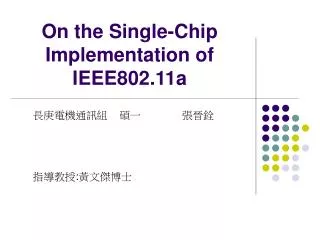
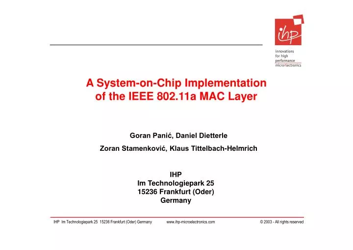
A System-on-Chip Implementation of the IEEE 802.11a MAC Layer. Goran Panić, Daniel Dietterle Zoran Stamenković, Klaus Tittelbach-Helmrich. Overview. Introduction Protocol Implementation Hardware/Software Partitioning System Architecture Components Description Synthesis Results

E N D
A System-on-Chip Implementationof the IEEE 802.11a MAC Layer Goran Panić, Daniel Dietterle Zoran Stamenković, Klaus Tittelbach-Helmrich
Overview • Introduction • Protocol ImplementationHardware/Software Partitioning • System ArchitectureComponents Description • Synthesis Results Estimated Area & Power • Layout ResultsFinal Design Results • Summary 2
Introduction • Functionality of the MAC described in the IEEE 802.11a standard • Wireless market Atheros, Intersil, Cisco, TI, … • Target: baseband, MAC and radio transcieving part integrated on a single chip • IHP MAC - designed as a complete solution on chip • Easy integration with the baseband 3
Design flow overview SDL model Protocol description Translation to C model Simulations & Measurements Performance investigation Hw/Sw partitioning VHDL model Hw Acc design System consideration Abstract and HDL level Architecture description Data preparation Logic and Layout Synthesis System implementation 4
Protocol Implementation SDL Model • Abstract protocol model • Generation of C model • Performance estimation in order to perform Hw/Sw partitioning 5
Hardware Accelerator Processor bus • executes timing critical MAC functions • Timers, CRC, RC4, address filter • reduction of power consumption • interface between baseband and CPU • completely modeled in VHDL • synthesized and simulated for 80MHz • 5x512B single-port memory • 2x256B dual-port memory • soft resetable Bus_Interface Timers Control MIB Tx Rx Channel_State CRC PHY_Interface CRC CRC RC4 On-chip RAM Baseband processor 6
System Architecture 2 MIPS 4KEp I C 2 I C EJTAG Core EC GPIO Hw X#1 EPP Acc EC-to-X Bus GPIO Controller X#0 Serial 0 Peripheral Bus UART 0 Controller UART 1 Serial 1 SRAM FLASH • complete rtl description in VHDL/Verilog • verification environment and synthesis scripts 7
System Architecture Components verification models 2 MIPS 4KEp I C 2 I C EJTAG Core EC GPIO Hw X#1 EPP Acc Test Environment EC-to-X Bus GPIO Controller X#0 Serial 0 Peripheral Bus UART 0 Controller UART 1 Serial 1 Test program Async RAM Async ROM • complete rtl description in VHDL/Verilog • verification environment and synthesis scripts 8
Synthesis Results Estimated Estimated Design name power area (%) (%) MIPS core 16.7 17 2 I C bus controller 0.3 0.4 UART x 2 2.7 3.5 EC-to-X bus controller 0.8 3.4 Peripheral bus 0.8 1.6 controller Accelerator core 14.1 15.9 Single-port RAM 512B x 5 41.6 49.7 Dual-port RAM 256B x 2 19.4 9.5 GPIO 0.8 1.3 Glue logic 0.2 0.3 Chip 100 100 9
System Layout • Facts • Technology: IHP 0.25μm CMOS • Area: ~ 30 mm2 • Number of gates: 420,000 NAND • Number of pins: 140 sig + 16 pow • Package: PQFP 208L 28*28*3.35P0.5 • Peak Power: ~1W at 80 MHz, 2.5V • Chip testing: • Successful on Agilent 93000 10
Summary Presented design flow provides: • Efficient and flexible modeling and implementation of a MAC protocol • Low power • High performance • Easy integration to a baseband processing unit What can be done in the future: • PCMCIA interface to TCP/IP layer (rev 1) • Custom connection to the baseband (rev 1) • Usage of high performance memory blocks (rev 1) • Clock gating • AMBA bus 11