Download
1 / 18
180 likes | 315 Views
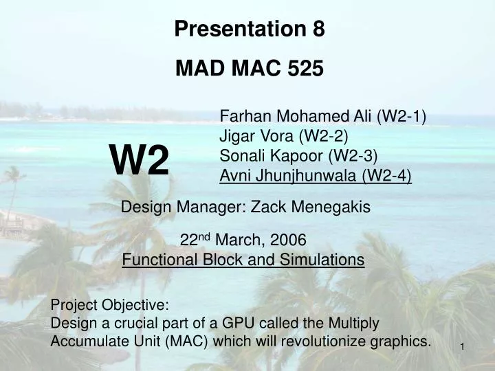
Presentation 8 MAD MAC 525. Farhan Mohamed Ali (W2-1) Jigar Vora (W2-2) Sonali Kapoor (W2-3) Avni Jhunjhunwala (W2-4). W2. Design Manager: Zack Menegakis. 22 nd March, 2006 Functional Block and Simulations. Project Objective:

E N D
Presentation 8 MAD MAC 525 Farhan Mohamed Ali (W2-1)Jigar Vora (W2-2)Sonali Kapoor (W2-3) Avni Jhunjhunwala (W2-4) W2 Design Manager: Zack Menegakis 22nd March, 2006 Functional Block and Simulations Project Objective: Design a crucial part of a GPU called the Multiply Accumulate Unit (MAC) which will revolutionize graphics.
MAD MAC 525 Status: • Project chosen • Specifications defined • Architecture • Design • Behavioral Verilog • Testbenches • Verilog : Gate Level Design • Floor plan • Schematics and Analog Verifications • Layout of basic gates and small blocks • Large block layouts, extractions, LVS, simulations (in progress) • Spring Break • To be done • Full chip layout and simulation
Block Diagram Input Input 16 Input 16 16 5 RegArray A RegArray B RegArray C 10 10 5 10 5 Multiplier Exp Calc Align 1 5 22 14 35 Control Logic & Sign Dtrmin Leading 0 Anticipator Adder/Subtractor 36 4 Normalize 14 1 5 Round Reg Y 1 10 5 15 16 Output 1 Ovf Checker
Design Decisions • Pipelining Stages: Add another stage in multiplier since adder is very fast. • Projected speed is at least 400 MHz • Exceeds the design goal of 300MHz
Pipelining Stages Reg C Multiplier Reg A Exp Calc Reg B Pipeline Reg Pipeline Reg Pipeline Reg Align C Pipeline Reg Pipeline Reg Adder Ld Zero Pipeline Reg Round Normalize Overflow checker Reg Y
Design Decisions • Pipelining Stages: Add another stage in multiplier since adder is very fast. • Projected speed is at least 400 MHz • Exceeds the design goal of 300MHz • Optimized adder design which implements carry look ahead architecture • Propagation delay of around 800ps (1250MHz) • Bit slicing the adder in the layout