Download
1 / 22
230 likes | 393 Views
0.37 mS/ m m In 0.53 Ga 0.47 As MOSFET with 5 nm channel and self-aligned epitaxial raised source/drain . Uttam Singisetti*, Mark A. Wistey, Greg J. Burek, Ashish K. Baraskar, Joel Cagnon, B. J. Thibeault, S. Stemmer, A.C. Gossard, and M.J.W. Rodwell ECE and Materials Departments

E N D
0.37 mS/mm In0.53Ga0.47As MOSFET with 5 nm channel and self-aligned epitaxial raised source/drain Uttam Singisetti*, Mark A. Wistey, Greg J. Burek, Ashish K. Baraskar, Joel Cagnon, B. J. Thibeault, S. Stemmer, A.C. Gossard, and M.J.W. Rodwell ECE and Materials Departments University of California, Santa Barbara, CA Eun Ji Kim, Byungha Shin, and Paul C McIntyre Materials Science and Engineering, Stanford University, Stanford, CA Yong-ju Lee Intel Corporation, Santa Clara, CA 2009 Device Research Conference Pennsylvania State University, State College, PA *uttam@ece.ucsb.edu
Outline • Motivation: III-V MOSFETs • Approach: Self-aligned source/drain by MBE regrowth • FET and contacts Results • Conclusion and future work
Why III-V MOSFETs • Silicon MOSFETs: • Gate oxide may limit <16 nm scaling Id / Wg ~ cox(Vg-Vth)vinj Id / Qtransit ~ vinj / Lg IBM 45nm NMOS Narayan et al, VLSI 2006 Alternative: In0.53Ga0.47As channel MOSFETs low m* (0.041 mo) → high injection velocity (~ 2×107 cm/s)* →increase drive current, decreased CV/I * Enoki et al , EDL 1990
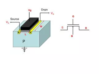
Target device structure Target 22 nm gate length Control of short-channel effects vertical scaling 1 nm EOT: thin gate dielectric, surface-channel device 5 nm quantum well thickness <5 nm deep source / drain regions ~3 mA/mm target drive current low access resistance self-aligned, low resisitivity source / drain contacts self-aligned N+ source / drain regions with high doping
Lg LS/D 22 nm InGaAs MOSFET: source resistance IBM High-k Metal gate transistor Image Source:EE Times • Source access resistance degrades Id and gm • IC Package density : LS/D ~ Lg =22 nm rc must be low • Need low sheet resistance in thin ~5 nm N+ layer • Design targets: rc ~1 W-mm2, rsheet ~ 400 W
22nm ion implanted InGaAs MOSFET Key Technological Challenges • Shallow junctions ( ~ 5 nm), high (~5×1019 cm-3)doping • Doping abruptness ( ~ 1 nm/decade) • Lateral Straggle ( ~ 5 nm) • Deep junctions would lead to degraded short channel effects
HAADF-STEM1* Interface 2 nm InGaAs MOSFET with raised source/drain by regrowth InGaAs regrowth InGaAs * TEM by J. Cagnon, Susanne Stemmer Group, UCSB Self-aligned source/drain defined by MBE regrowth1 Self-aligned in-situ Mo contacts2 Process flow & dimensions selected for 22 nm Lg design; present devices @ 200 nm gate length 1Wistey, EMC 2008 2Baraskar, EMC 2009
Regrown S/D process: key features Self-aligned & low resistivity ...source / drain N+ regions ...source / drain metal contacts Vertical S/D doping profile set by MBE abrupt on ~ 1 nm scale Gate-first gate dielectric formed after MBE growth uncontaminated / undamaged surface
Process flow* * Singisetti et al; Physica Status Solidi C, vol. 6, pp. 1394,2009
Key challenge in S/D process: gate stack etch Requirement: avoid damaging semiconductor surface: Approach: Gate stack with multiple selective etches* FIB Cross-section Damage free channel SiO2 Cr W Process scalable to sub-100 nm gate lengths * Singisetti et al; Physica Status Solidi C, vol. 6, pp. 1394,2009
Key challenge in S/D process: dielectric sidewall Sidewall must be kept thin: avoid carrier depletion, source starvation. • Target < 15 nm sidewall in 22 nm Lg device • 20-25 nm SiNx thick sidewalls in present devices • Pulse doping in the barrier: compensate for carrier depletion from Dit
MOSFET SEMs Cross-section after regrowth, but before Mo deposition Cross-section after regrowth, but before Mo deposition Cross-section after regrowth, but before Mo deposition Top view of completed device Top view of completed device
MOSFET characteristics 4.7 nm Al203 , 1×1013 cm-2 pulse doping • Maximum Drive current (Id): 0.95 mA/mm • Peak transconductance (gm): 0.37 mS/mm Id and gm below expected values
FET source resistance SEM InGaAs regrowth on unprocessed thin InP* • Series resistance estimated by extrapolating Ron to zero gate length • Source access resistance ~ 500 W-mm
Source resistance : regrowth TLMs SEM SEM InGaAs regrowth FET Regrowth TLMs W / Cr / SiO2 gate No regrowth • TLMs fabricated on the regrowth far away from the gate • Regrowth sheet resistance ~ 29 W • Mo/InGaAs contact resistance ~ 5.5 W-mm2 (12.6 W-mm) TLM data does not explain 500 W-mm observed FET source resistance
Source resistance: electron depletion near gate R1 R2 • Electron depletion in regrowth shadow region (R1 ) • Electron depletion in the channel under SiNx sidewalls (R2 )
InAsregrowth Gate InAs source/drain regrowth top of gate side of gate Mo S/D metal with N+ InAs underneath Improved InAs regrowth with low As flux for uniform filling1 InAs less susceptible to electron depletion: Fermi pinning above Ec2 1 Wistey et al, EMC 2009 Wistey et al NAMBE 2009. 2Bhargava et al , APL 1997
InAs S/D E-FET DC characteristics 4.7 nm Al203, InAs S/D E-FET
Subthreshold characteristics • Ion/Ioff~ 104:1
Drive current and transconductance 0.95 mA/mm peak Id , ~0.45 mS/mm peak gm
Source-drain access resistance* • Ron = 600 W-mm for Lg=0.2 mm so Rs< 300 W-mm • Rs is too small to explain observed gm or Id *Wistey et al, NAMBE 2009
Conclusion • Self-aligned raised source/drain for scaled channel ( 5nm) • D-FETs: peak Id = 0.95 mA/mm, and peak gm =0.37 mS/mm • InAs Source/Drain E-FETs: peak Id= 0.95 mA/mm and peak gm= 0.45 mS/mm • Next: scale to ~50 nm Lg gate dielectric quality This work was supported by Semiconductor Research Corporation under the Non-classical CMOS Research Program