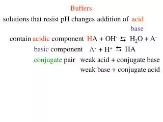

Buffers
E N D
Presentation Transcript
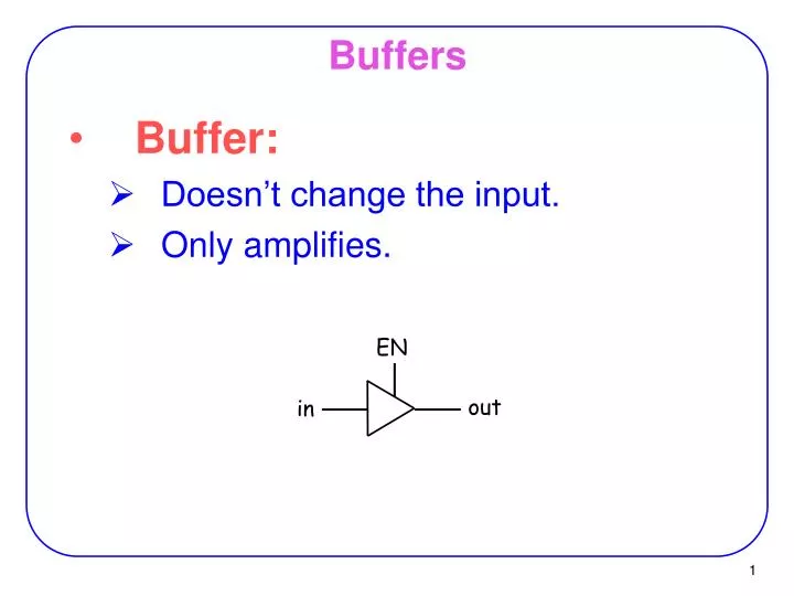
Buffers • Buffer: • Doesn’t change the input. • Only amplifies. EN out in
Three-State Buffers • Buffer output has 3 states: 0, 1, Z • Z stands for High-Impedance Open circuit EN = 0 out = Z (open circuit) EN = 1 out = in (regular buffer) EN out in
Three-state buffer(BUF)/inverter(INV) symbols EN EN out out in in 3-state BUF, EN high 3-state INV, EN high EN EN out out in in 3-state BUF, EN low 3-state INV, EN low
Open Collector/Drain Gates • Outputs of two (or more) gates must not be wired together: A If A = B out = A = B If A B a large enough current can be created, that causes excessive heating and could damage the circuit. out B wired
ENA A out ENB B S A 0 out B 1 S Multiplexed output lines using three-state buffers A B
Open Collector/Drain Gates • Outputs of some gates can be wired: • The result: O1 AND O2 • Open Collector Gates in TTL Technology • Open Drain Gates in CMOS Technology O1 A O1 . O2 Out = B O2
Open Collector/Drain Gates • Open Collector (Open Drain) NAND Truth Table: • Z (Hi-Z) (Hi-Impedance): • As if it is unconnected. OD • The gate cannot pull up the output • needs a resistor to pull it up if an input is ‘0’
Open-collector NAND gate Open Collector/Drain Gates • Wired AND: If A and B are "1", output is actively pulled low if C and D are "1", output is actively pulled low if one gate is low, the other high, then low wins if both gates are "1", the output floats, pulled high by resistor Hence, the two NAND functions are AND'd (wired) together! Pull-up resistor F 0 V C D OD OD
NAND-Only Implementation • Find Sum-of-Product form. • Inventers can be added • Equivalent NAND-only
Use Open Collector/Drain NAND Gates: OD OD OD NAND-Only Implementation • NAND = AND + NOT
Another Method • Instead of finding the circuit for F, find the circuit for F’ in the first stage • Then there will be no Inverter at the output OD OD OD • Wired OR: • Open drain/collector gate with active low inputs.