Download
1 / 110
1.19k likes | 1.48k Views
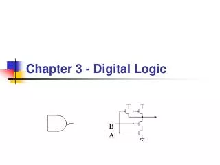
B. A. Chapter 3 - Digital Logic. Success is not the key to happiness. Happiness is the key to success. If you love what you are doing, you will be successful. Concepts to Learn…. The Transistor Devices: Inverter, NAND, NOR, Drivers De Morgan’s Law Translations

E N D
B A Chapter 3 - Digital Logic
Success is not the key to happiness. Happiness is the key to success. If you love what you are doing, you will be successful. Chapter 3 - Digital Logic
Concepts to Learn… • The Transistor • Devices: Inverter, NAND, NOR, Drivers • De Morgan’s Law • Translations • Decoders, Multiplexors, Adders, PLAs • Logical Completeness • Sequential Logic • Latches • Memory • Finite State Machine Chapter 3 - Digital Logic
The Transistor History of the Transistor • Around 1945, Bell Labs scientists discovered that silicon was comprised of two distinct regions differentiated by the way in which they favored current flow. • The area that favored positive current flow they named "p" and the area that favored negative current flow they named "n". Chapter 3 - Digital Logic
The Transistor The Transistor Effect • The transistor effect describes the change from a condition of conductivity (switched “on”, full current flow) to a condition of insulation (switched “off”, no current flow). Chapter 3 - Digital Logic
The Transistor Digital Logic Circuits • Computers = large number of simple structures • Intel 4004 = 2,300 transistors • Intel Pentium 4 = 42 million transistors • Intel Core 2 Duo = 291 million transistors • Intel i7 “Bloomfield” = 731 million transistors Chapter 3 - Digital Logic
The Transistor Moore’s Law 2000’s 1990’s 1980’s 1970’s 1960’s 1950’s 1947 Moore’s Law: The number of transistors per area doubles every 1.5 - 2 years. Early 1900’s Chapter 3 - Digital Logic
gate gate current flow current flow P-type Transistor N-type Transistor gate FET 0 on 1 off gate FET 0 off 1 on The Transistor The MOS Transistor • A transistor acts like a switch • conducts current only when "on" Off = open circuit On = closed circuit complementary MOS = metal-oxide semiconductorCMOS = complementary MOS with both N and P transistors Chapter 3 - Digital Logic
S S G G D D The Transistor Field Effect Transistor P type N type Gate = Ground = ‘0’ Chapter 3 - Digital Logic
S S G G D D The Transistor Field Effect Transistor Operation P type N type Gate = Vcc = ‘1’ Chapter 3 - Digital Logic
The Transistor CMOS Gates We want complementary pull-up and pull-down logic: the pull-down is “on” when the pull-up is “off”, and visa-versa. Pullup Structure F Complementary Pulldown Structure The “C” in CMOS Even in the digital world "EVERYTHING IS ANALOG"! Chapter 3 - Digital Logic
1 1 1 on off 0 1 in out 1 0 on off 0 0 0 This is a truth-table. It tells what the output will be for all combinations of the inputs. in out 0 1 1 0 Symbols are abstractions! Inverter Symbols Digital Logic Devices The Inverter Chapter 3 - Digital Logic
1 1 1 a 0 0 on on b 0 1 on off nor 1 0 off off on off 0 0 0 0 0 0 a b nor 0 0 1 0 1 0 1 0 0 1 1 0 NOR Symbols Digital Logic Devices The NOR Gate (NOT-OR) Chapter 3 - Digital Logic
a a or or b b 0 a b or 0 0 0 0 1 1 1 0 1 1 1 1 OR Symbol Digital Logic Devices The OR Gate • How do you build an OR gate? Chapter 3 - Digital Logic
1 1 1 1 on off off off 1 0 1 1 on on 1 0 on off 0 0 a b nand 0 0 1 0 1 1 1 0 1 1 1 0 NAND Symbols Digital Logic Devices The NAND Gate (NOT-AND) 1 1 NAND b a 0 Chapter 3 - Digital Logic
a and b AND b a a b AND 0 0 0 0 1 0 1 0 0 1 1 1 AND Symbol Digital Logic Devices The AND Gate • How do you build an AND gate? Chapter 3 - Digital Logic
? ? Pullup Structure F Pulldown Structure Digital Logic Devices Why Inverting Logic? • Why can’t we use • N transistors to pull up to Vcc, and • P transistors to pull down to ground? • Because • N transistors do not pass good voltage levels for 1’s • P transistors do not pass good voltage levels for 0’s • It just doesn’t work electronically! So… • Only use P transistors in pull-up structures! • Only use N transistors in pull-down structures! Chapter 3 - Digital Logic
Digital Logic Devices Drivers • Why can’t we use CMOS transistors to connect to a bus? • P transistors to pull up to Vcc, and • N transistors to pull down to ground • Because connecting Vcc to ground let’s the magic smoke out! • Solution: Tri-state driver Chapter 3 - Digital Logic
De Morgan’s Law De Morgan’s Law To distribute the bar, change the operation. NOR Symbols NAND Symbols Chapter 3 - Digital Logic
0 0 0 1 1 1 1 0 1 1 0 1 0 0 1 0 1 0 0 1 0 1 1 1 0 0 0 0 De Morgan’s Law De Morgan’s Proof Chapter 3 - Digital Logic
It’s just a NAND gate drawn a different way!!! Translations Reading Functions from Symbols The output will be high if any of the inputs are low... The output will be low if all of the inputs are high... a b out 0 0 1 0 1 1 1 0 1 1 1 0 The output will be high if the first input is low OR the second input is high... Chapter 3 - Digital Logic
Translations You Should Know How to Translate These are three different ways of representing logical information LogicEquations You can convert any one of them to any other LogicGates TruthTables Chapter 3 - Digital Logic
s y a b y Translations From Equations to Gates y = NOT(s) AND a AND NOT(b) Chapter 3 - Digital Logic
out Translations From Equations to Gates y = (~s a ~b) + (~s a b) + (s a b) + (s ~a b) Chapter 3 - Digital Logic
Translations From Truth tables to Gates • Each row of truth table is an AND gate • Each output column is an OR gate When we write s we mean the inverse of s or s after it has gone through an inverter. s s a b out 0 0 0 0 0 0 1 0 0 1 0 1 0 1 1 1 1 0 0 0 1 0 1 1 1 1 0 0 1 1 1 1 a b s a b out s a b s a b Chapter 3 - Digital Logic
OR OR OR s a b Translations From Truth table to Equations • Write out truth table a combination of AND’s and OR’s • equivalent to gates • easily converted to gates out = s a b out 0 0 0 0 0 0 1 0 0 1 0 1 0 1 1 1 1 0 0 0 1 0 1 1 1 1 0 0 1 1 1 1 Chapter 3 - Digital Logic
OR OR Contains a don’t care - out is independent of b There is a whole field of boolean minimization that capitalizes on this property. You will learn this in the next class... OR OR Translations From Equations to Truth Tables • For each AND term • fill in the proper row on the truth table s a b out 0 0 0 0 0 0 1 0 0 1 0 1 0 1 1 1 1 0 0 0 1 0 1 1 1 1 0 0 1 1 1 1 s a b out 0 0 0 0 0 0 1 0 0 1 0 1 0 1 1 1 1 0 0 0 1 0 1 1 1 1 0 0 1 1 1 1 Chapter 3 - Digital Logic
Translations Manipulating Logic Expressions Laws (basic identities) of Boolean algebra. Chapter 3 - Digital Logic
2-to-4 Decoder W X Y A W Z B X A B Y DECODERSymbol Z Circuits Decoders • Decode the input and signify its value by raising just one of its outputs. 1 if A,B = 00 1 if A,B = 01 1 if A,B = 10 1 if A,B = 11 Chapter 3 - Digital Logic
A W B X Y Z Circuits Decoders • Write the truth table A B W X Y Z 0 0 0 1 1 0 1 1 1 0 0 0 0 1 0 0 0 0 1 0 0 0 0 1 Chapter 3 - Digital Logic
A B S A B 0 1 S C C Symbols are abstractions! MULTIPLEXOR Symbol Circuits Multiplexors • Connect one of its inputs to its output according to select signals • Useful for selecting one from a collection of data inputs. • Usually has 2n inputs and n select lines. Chapter 3 - Digital Logic
A B S C 0 X 0 0 1 X 0 1 X 0 1 0 X 1 1 1 A B 0 1 S C Circuits Multiplexors • Write the truth table A simpler way… A B S C 0 0 0 0 0 0 1 0 0 1 0 0 0 1 1 1 1 0 0 1 1 0 1 0 1 1 0 1 1 1 1 1 Chapter 3 - Digital Logic
b3 a3 b2 a2 b1 a1 b0 a0 Full Adder Full Adder Full Adder Full Adder ‘0’ c3 c2 c1 c0 s3 s2 s1 s0 Circuits Adders • At each digit position add together the 2 operands and the carry-in c 0110 +0101 1011 • Just like longhand addition • except it’s in binary... Chapter 3 - Digital Logic
Circuits Full Adder Module Design a b c cyout sum 0 0 0 0 0 0 0 1 0 1 0 1 0 0 1 0 1 1 1 0 1 0 0 0 1 1 0 1 1 0 1 1 0 1 0 1 1 1 1 1 Chapter 3 - Digital Logic
? ? ? ? ? ? ? ? ? ? ? ? ? ? ? ? ? ? ? ? ? ? ? ? ? ? ? PLAs Programmable Logic Arrays • Programmable Logic Array (PLA) can be used to implement any logic function • Take truth table of any logic function • Convert into equation (any truth table can be expressed as set of “and” expressions “or”ed together) • PLA programmed by making/breaking wire connections Outputs: Inputs: Chapter 3 - Digital Logic
? ? Out1 = ABC + ABC + ABC ? ? ? ? ? ? ? Out1 Out2 A B C Out1 Out2 Out3 Out3 ? ? ? 0 0 0 0 1 1 ? ? ? 0 0 1 1 0 0 ? ? ? Outputs 0 1 0 0 1 0 ? ? ? ? ? ? 0 1 1 0 0 0 Inputs ? ? ? 1 0 0 1 0 0 A 1 0 1 0 1 0 1 1 0 0 0 0 B 1 1 1 1 0 1 C PLAs PLA Example Out2 = ABC + ABC + ABC Out3 = ABC + ABC Chapter 3 - Digital Logic
AND gate, INVERTER • OR can be replaced by an AND and three INVERTERS DeMorgan’s Theorem • OR gate, INVERTER • AND can be replaced by an OR and three INVERTERS DeMorgan’s Theorem Logical Completeness Logical Completeness What is the minimum set of gate types needed to implement any logic function? • AND gate, OR gate, INVERTER Chapter 3 - Digital Logic
Logical Completeness Logical Completeness • NAND • INVERTER • AND • OR NAND (by itself) is logically complete if you can implement an INVERTER, AND, and OR gate using only NAND gates. Chapter 3 - Digital Logic
4 1 8 4 30 25 5 20 10 15 Sequential Success depends onthe sequence of values (e.g, R-13, L-22, R-3). Sequential Logic Combinational vs. Sequential • Two types of “combination” locks Combinational Success depends only onthe values, not the order in which they are set. Chapter 3 - Digital Logic
Sequential Logic Storage Elements • Everything so far is called combinational • the output is strictly a function of the current inputs • Real computing systems need storage • for holding previously computed values • for remembering its place (state) in the middle of a multi-step operation • Storage elements remember what was stored in them for later retrieval using feedback Chapter 3 - Digital Logic
This is a stable state – it will sit like this forever This is also a stable state – it will sit like this forever 1 0 1 Sequential Logic Bi-Stability = Key to Memory 0 1 0 When there are 2 stable states - a bi-stable circuit… Chapter 3 - Digital Logic
Sequential Logic RS Latch • Signals s and r are active low • they change the circuit when they go low • Output q goes high when s goes low • Output q goes low when r goes low • Output q remains the same otherwise s s s q q q Cross-coupled NAND gates Note the feedback same same q q q r r r Chapter 3 - Digital Logic
Sequential Logic RS Latch – Bi-Stable Circuit s s q 1 1 q 1 0 q q 0 1 r r 1 1 This is also a stable state – it will sit like this forever This is a stable state – it will sit like this forever Chapter 3 - Digital Logic
0 1 1 1 0 1 1 0 0 1 0 0 1 1 1 1 0 1 Sequential Logic RS Latch (continued) s q q r 1 1 Chapter 3 - Digital Logic
Sequential Logic RS Latch : Next State Table • Defines output as a function of inputs (s and r) and current output (q, its state) s r q qnext 0 0 0 x 0 0 1 x 0 1 0 1 0 1 1 1 1 0 0 0 1 0 1 0 1 1 0 q 1 1 1 q not allowed set reset keep old state Chapter 3 - Digital Logic
d s q WE D Q D-Latch we q r Latch Gated D Latch • Output q gets value from input d only when we is high • we stands for write enable, think of it as a load signal LATCH Symbol Symbols are abstractions! Chapter 3 - Digital Logic
Quiz 1. What is a bi-stable circuit? 2. Draw a logic circuit (using N and P type transistors) for a 3 input NAND gate. 3. With a RS NAND latch, why can’t R and S be low at the same time? 4. How is Q set with the following latch? Chapter 3 - Digital Logic
Quiz (Answers) 1. What is a bi-stable circuit? • When the circuit has 2 stable states 2. Draw a logic circuit (using N and P type transistors) for a 3 input NAND gate. Chapter 3 - Digital Logic
Quiz (Answers) 3. With a RS NAND latch, why can’t R and S be low at the same time? • This state would force both outputs to a logic 1, overriding the feedback latching action. • Outputs Q and Q' must have opposite logic levels. • Results in a “race” condition – final state of the latch cannot be determined. Chapter 3 - Digital Logic