NUMERICAL EXAMPLES FOR EE213 Part II
240 likes | 567 Views
NUMERICAL EXAMPLES FOR EE213 Part II. 1) Determine the r’ e of a transistor that is operating with I E = 5 mA. r’ e = 25 mV/ I E = 25 mV/ 5 mA = 5 W. 2) For the CE amplifier , R 1 = 33 k W , R 2 = 8.2 k W , R C = 2.7 k W ,

NUMERICAL EXAMPLES FOR EE213 Part II
E N D
Presentation Transcript
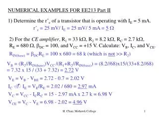
NUMERICAL EXAMPLES FOR EE213 Part II 1) Determine the r’e of a transistor that is operating with IE = 5 mA. r’e = 25 mV/ IE = 25 mV/ 5 mA = 5W 2) For the CE amplifier, R1 = 33 kW, R2 = 8.2 kW, RC = 2.7 kW, RE = 680 W, bDC = 100, and VCC = +15 V. Calculate: VB, IC, and VCE. RIN(base) = bDCRE = 100 x 680 = 68 k (which is not >> R2) VB = (R2//RIN(base))VCC /(R1+R2//RIN(base)) = (8.2//68)x15/(33+8.2//68) = 7.32 x 15 / (33 + 7.32) = 2.72 V VE = VB - VBE = 2.72 - 0.7 = 2.02 V IC IE = VE/RE = 2.02 / 680 = 2.97 mA VC = VCC - ICRC = 15 - 2.97 mA x 2.7 k = 6.98 V VCE = VC - VE = 6.98 - 2.02 = 4.96 V H. Chan; Mohawk College
3) For the circuit in e.g. 2, what are Rin(tot), Rout, and Av if bac = 120, and RL = 1 kW? Rin(base) = bacr’e= 120 x 25 mV / IE = 120 x 25 / 2.97 = 1.01 kW Rin(tot) = R1//R2//Rin(base) = 33k//8.2k//1.01k = 875.4W Rout= RC//RL = 2.7k // 1k = 729.7W Av = -Rc / r’e = -729.7 / (25/2.97) = -86.7 4) If a 50 mV, 200 W source is connected to the circuit in e.g. 2 & 3, determine: Vb, A’v, and Vout Vb = Rin(tot)Vs/(Rs+Rin(tot)) = 875.4 x 50 mV/(200+875.4) = 40.7 mV A’v = Rin(tot)Av/(Rs+Rin(tot)) = 875.4 x (-86.7)/(200+875.4) = -70.6 Vout = A’vVin or AvVb = -70.6 x 50 mV = -3.53 V 5) What is the minimum value of CE in e.g. 2 if the amplifier operates over a frequency range from 500 Hz to 100 kHz. XCRE/10 = 68 W; CE 1/(2pfminXC) = 4.68mF H. Chan; Mohawk College
6) For the swamped CE amplifier with R1 = 10 kW, R2 = 2 kW, RC = 4.7 kW, RE1 = 150 W, RE2 = 470 W, VCC = 12 V, and bDC = 110, bac = 125, calculate: Av, and Rin(tot) RIN(base) = bDC(RE1+RE2) = 110 x (150+470) = 68.2 k >> R2 VB R2VCC/(R1+R2) = 2 x 12 / (10 + 2) = 2 V VE = VB - 0.7 = 1.3 V; IE = VE / (RE1+RE2) = 2.1 mA r’e = 25 mV/ IE = 25 / 2.1 = 11.9 W (which is << RE1) Av -RC / RE1 = -4.7k / 150 = -31.3 Rin(base) = bac(r’e+RE1) = 125 x (11.9 + 150) = 20.24 kW Rin(tot) = R1//R2//Rin(base) = 10k//2k//20.24k = 1.54 kW 7) If a 0.5 V, 300 W source is connected to the circuit in e.g. 6, and RL = 1 kW, find A’v. Av = -(RC//RL) /RE1 = -4.7k//1k / 150 = -5.5 A’v = Rin(tot)Av/(Rin(tot)+Rs) = 1.54k x (-5.5)/(1.54k+300) = -4.6 H. Chan; Mohawk College
8) For the emitter-follower amplifier, R1 = 27 kW, R2 = 10 kW, RE = 1.2 kW, RL = 2 kW, bDC = 120, VCC = 15 V. Find: IC, and VCE. VBR2VCC/(R1+R2) = 10 x 15 /(27+10) = 4.05 V VE = VB - 0.7 = 4.05 - 0.7 = 3.35 V; IC VE/RE = 3.35/1.2k = 2.8 mA VCE = VC - VE = VCC - VE = 15 - 3.35 = 11.65 V 9) If bac = 85 for e.g. 8, and a 2 V, 300 W source is connected to the input, determine: Rin(tot), Rout, Av, and Ai. r’e = 25 mV/ IE = 25 / 2.8 = 8.93 W; Re = RE//RL = 1.2k//2k = 750 W Rin(base) = bac(r’e+Re) = 85 x (8.93+750) = 64.5 kW Rin(tot) = R1//R2//Rin(base) = 27k//10k//64.5k = 6.56 kW Rout (Rs/bac) //Re = (300/85) // 750 = 3.5W Av = Re/(r’e+Re) = 750/(8.93+750) = 0.988 Ie = Vout/Re = AvVb/Re = AvRin(tot)Vin/((Rs+Rin(tot))Re) = 2.52 mA Iin = Vin/Rin(tot) = 2/6.56k = 0.3 mA; Ai = Ie/Iin = 2.52 / 0.3 = 8.4 H. Chan; Mohawk College
10) For e.g. 8 & 9, if the transistor is replaced by a Darlington pair where bDC = bac = 100, and RE = RL = 8 W, find: Av, and Rin(tot). RIN(base) = b2DCRE = 1002 x 8 = 80 kW VB = (R2//RIN(base)VCC) / (R1+R2//RIN(base)) = 3.72 V VE2 = VB-2VBE = 3.72 - 2x0.7 = 3.02V; IE = VE2/RE = 377.5 mA r’e = 25 mV/IE = 25 / 377.5 = 66.2 mW; Re = RE//RL = 8//8 = 4 W Av = Re/(Re+r’e) = 0.984 Rin(base) = b2ac(r’e+Re) = 1002 x (0.0662 + 4) = 40.66 kW 11) Find Rin, Av, and Ap for a CB amplifier with R1 = 68 kW, R2 = 15 kW, RC = 3.3 kW, RE = 1.5 kW, RL = 5 kW, VCC = 24 V, bDC = 180. VB R2VCC / (R1+R2) = 4.34 V; VE = VB - 0.7 = 3.64 V IE = VE/RE = 2.43 mA; Rin r’e = 25 mV/IE = 10.3W Av = Rc/r’e = (RC//RL)/r’e = (3.3k//5k) / 10.3 = 193 Ap Av = 193 H. Chan; Mohawk College
12) A 30 dB amplifier is cascaded with a 20 dB amplifier. Calculate their overall gain in dB. What would be the output voltage at the 2nd amplifier if the input voltage to the 1st amplifier is 20 mV? AvT = 30 + 20 = 50 dB; the gain in non-dB value is 316.2 Vout = AvTVin = 316.2 x 20 mV = 6.32 V 13) Two capacitively-coupled CE amplifier stages have the following components: R1 = R5 = 56 kW, R2 = R6 = 12 kW, R3 = R7 = 3.6 kW, R4 = R8 = 1 kW, RL = 2 kW, VCC = 20 V, bDC = bac = 140 for Q1 and Q2. Find AvT DC voltages and currents for both stages are the same: VB R2VCC /(R1+R2) = 3.53 V; VE = VB - 0.7 = 2.83 V IE = VE/R4 = 2.83 mA; r’e = 25 mV/IE = 8.83 W Rc1 = R3//R5//R6//Rin(base2) = 3.6k//56k//12k//(140x8.83) = 841.8 W Av1 = Rc1/r’e = 95.3; Av2 = Rc2/r’e = (R7//RL)/r’e = 145.6 AvT = Av1Av2 = 13,876 or 82.85 dB H. Chan; Mohawk College
IC(mA) 8.63 6.82 Q VCE 0 12 V 6.21 V 14) For a CE amplifier with R1 = 12 kW, R2 = 5.6 kW, RC = 1.2 kW, RE = 560 W, RL = 1.8 kW, VCC = 12 V, and bDC = bac = 110, draw the dc and ac load lines. Obtain all the important parameters for the lines. VBQ R2VCC/(R1+R2) = 3.82 V; VEQ = VBQ - 0.7 = 3.12 V ICQ IEQ = VEQ/RE = 3.12 / 560 = 5.57 mA VCQ = VCC - ICQRC = 12 - 5.57 mA x 1.2 k = 5.32 V VCEQ = VCQ - VEQ = 2.2 V IC(sat) = VCC/(RC+RE) = 6.82 mA VCE(cutoff) = VCC = 12 V Rc = RC//RL = 720 W Vce(cutoff) = VCEQ + ICQRc = 6.21 V Ic(sat) = ICQ+VCEQ/Rc = 8.63 mA H. Chan; Mohawk College
15) Determine the value of RE so that the Q-point in e.g. 14 is approximately centred on the ac load line At mid-point of the ac load line, ICQ = Ic(sat)/2= 8.63/2 = 4.32 mA and VCEQ = Vce(cutoff)/2 = 6.21/2 = 3.11 V Since VCEQ = VCC - ICQ(RC+RE) RE = (VCC - VCEQ - ICQRC) / ICQ = 858W 16) Calculate a) the min. transistor power rating, b) the max.ac output power without distortion, c) the efficiency for e.g. 14. PD(min) = PDQ = VCEQICQ = 2.2 x 5.57 mA = 12.3 mW Since the Q-point is closer to saturation, the max. voltage swing is VCEQ, and the corresponding max. current swing is VCEQ/Rc Max. Pout = Vout(rms)Iout(rms) = 0.707VCEQ(0.707VCEQ/Rc) = 3.36 mW PDC = VCCICQ = 12 x 5.57 mA = 66.8 mA So, h = Pout / PDC = 3.36 / 66.8 = 0.05 or 5% H. Chan; Mohawk College
17) Determine the dc voltages at the bases and emitters of the matched complementary transistors Q1 and Q2 of the class AB amplifier with R1 = R2 = 120 W, and VCC = 24 V. Also determine VCEQ for each transistor. Assume VD1 = VD2 = VBE = 0.7 V The total current through R1, D1, D2, and R2 is IT = (VCC-VD1-VD2)/(R1+R2) = (24-0.7-0.7)/(120+120) = 94.2 mA VB1 = VCC - ITR1 = 24 - 94.2 mA x 120 = 12.7 V VB2 = VB1 - VD1 - VD2 = 12.7 - 0.7 - 0.7 = 11.3 V VE1 = VE2 = VB1 - VBE = 12.7 - 0.7 = 12 V VCEQ1 = VCEQ2 = VCC / 2 = 24/2 = 12 V 18) If RL = 8 W, bac = 120, and r’e = 5 W for e.g. 17, find: Iout(pk) and Rin. Iout(pk)= Ic(sat) = VCEQ / RL = 24/8 = 3 A Rin = bac(r’e + RL) = 120 (5 + 8) = 1.56 kW H. Chan; Mohawk College
19) Find the max. Pout, the dc input power, and h for e.g. 17 & 18. Max. Pout = 0.25VCCIc(sat) = 0.25 x 24 x 3 = 18 W PDC = VCCIc(sat) / p = 24 x 3 / p = 22.92 W h = Pout / PDC = 18 / 22.92 = 0.785 or 78.5% 20) If the circuit in e.g. 17 & 18 is replaced by a Darlington class AB push-pull amplifier with bac1 = bac2 = 55, find Rin. Rin = btot (r’e + RL) = 552 (5 + 8) = 39.3 kW 21) A tuned class C amplifier has a VCC = 12 V, VCE(sat) = 0.2 V, IC(sat) = 120 mA, Rc = 80 W, and a duty cycle of 15%, determine: PD(avg), and efficiency assuming max. output power operation. PD(avg) = (tON/T)VCE(sat)IC(sat) = 0.15 x 0.2 x 120 mA = 3.6 mW Max. Pout = 0.5V2CC / Rc = 0.5 x 122 / 80 = 900 mW h = Pout / (Pout + PD(avg) ) = 900 / (900 + 3.6) = 0.996 or 99.6 % H. Chan; Mohawk College
RD 22) If VGS(off) = -5 V, IDSS = 10 mA, and RD = 1 kW, what is the min. value of VDD to put the JFET in constant-current region of operation. ID VDD Since VGS = 0, VGS(off) = -VP = -5, I.e. VP = 5 V, and ID = IDSS = 10 mA So, min. VDS = VP = 5 V Min. VDD = VD(min) + IDRD = 5 + 10 mA x 1k = 15 V 23) What is the value of gm0 for the JFET in e.g. 22? gm0 = 2IDSS / |VGS(off)| = 2 x 10 mA / 5 = 4 mS 24) Determine ID, gm, and RIN for e.g. 22 when VGS = -2 V, and IGSS = -0.2 nA. ID = IDSS (1 - VGS/VGS(off))2 = 10 (1 - (-2/-5))2 = 3.6 mA gm = gm0(1-VGS/VGS(off)) = 4 mS (1 - (-2/-5)) = 2.4 mS RIN = |VGS/IGSS| = 2/0.2 nA = 10 GW H. Chan; Mohawk College
25) Find VDS and VGS for the circuit when RG = 10 MW, RD = 1.5 kW, RS = 330 W, VDD = 20 V, and ID = 4 mA. +VDD VS = IDRS = 4 mA x 330 = 1.32 V RD VG = 0 VD = VDD - IDRD = 20 - 4 mA x 1.5k = 14 V VDS = VD - VS = 14 - 1.32 = 12.68 V RG RS VGS = VG - VS = 0 - 1,32 = -1.32 V 26) Find RS to self-bias the JFET circuit where IDSS = 15 mA, VGS(off) = -7 V, and VGS is to be -2.5 V. ID = IDSS(1-VGS/VGS(off))2 = 15 mA(1-(-2.5/-7))2 = 6.2 mA RS = |VGS/ID| = 2.5 / 6.2 mA = 403W 27) Determine RD and RS for midpoint bias where IDSS = 15 mA, VDD = 20 V, and VGS(off) = -7 V. For midpoint bias, VD = VDD /2 = 10 V, and ID = IDSS /2 = 7.5 mA H. Chan; Mohawk College
27) cont’d VGS = VGS(off)/3.4 = - 7/3.4 = -2.06 V So, RS = |VGS/ID| = 2.06 / 7.5 mA = 275W RD = (VDD - VD) / ID = (20 - 10) / 7.5 mA = 1.33 kW 28) Find ID and VGS for the JFET circuit with voltage-divider bias given R1 = 5.6 MW, R2 = 1 MW, RD = 4.7 kW, RS = 2.7 kW, VDD = 15 V, and VD = 8 V. ID = (VDD - VD) / RD = (15 - 8) / 2.7k = 2.6 mA VS = IDRS = 2.6 mA x 2.7 k = 7 V VG = R2VDD/(R!+R2) = 1 x 15/(5.6 + 1) = 2.27 V VGS = VG - VS = 2.27 - 7 = - 4.63 V 29) A D-MOSFET has VGS(off) = -6 V, IDSS = 14 mA and VGS = 2 V. Find ID. What mode is it operating in? ID = IDSS(1-VGS/VGS(off))2 = 14(1- 2/(-6))2 = 24.9 mA Enhancement mode. H. Chan; Mohawk College
30) For an E-MOSFET, ID = 400 mA at VGS = 8 V, and VGS(th) 1 V. Determine ID for VGS = 4 V. K = ID / (VGS - VGS(th))2 = 400 mA /(8 - 1)2 = 8.16 mA/V2 ID = K(VGS - VGS(th))2 = 8.16 mA (4 - 1)2 = 73.4 mA 31) Determine VDS for a D-MOSFET with zero-bias, RD = 910 W, VDD = 20 V, VGS(of) = -6 V, and IDSS = 15 mA. For zero-bias, ID = IDSS = 15 mA VDS = VDD - IDRD = 20 - 15 mA x 910 = 6.35 V 32) If the E-MOSFET from e.g. 30 is used in a circuit with voltage- divider bias where R1 = 200 kW, R2 =40 kW, RD = 180 W, and VDD = 24 V, determine VGS and VDS. VGS = R2VDD / (R1+R2) = 40 x 24 / (200 + 40) = 4 V As found in e.g 30, when VGS = 4 V, ID = 73.4 mA Therefore, VDS = VDD - IDRD = 24 - 73.4 mA x 180 = 10.8 V H. Chan; Mohawk College
33) Determine ID for an E-MOSFET in a circuit with drain-feedback bias, RG = 10 MW, RD = 2.2 kW, VGS = 5 V, and VDD = 20 V. With drain-feedback bias, VDS = VGS = 5 V ID = (VDD - VDS) / RD = (20 - 5) / 2.2 k = 6.82 mA 34) The values for a CS self-biased JFET amplifier are: RG = 10 MW, RD = 1.2 kW, RS = 680 W, IDSS = 10 mA, VGS(off) = -6 V, VDD = 15 V, and Vin = 2 V. Assuming midpoint biasing, find: VDS and Vout. For midpoint biasing, ID = IDSS / 2 = 10 /2 = 5 mA VDS = VDD - ID(RD+RS) = 15 - 5 mA(1.2k+680) = 5.6 V VGS = - IDRS = - 5 mA x 680 = - 3.4 V gm0 = 2IDSS / |VGS(off)|= 2 x 10 mA/6 = 3333 mS gm = gm0(1-VGS/VGS(off)) = 3333 mS(1- 3.4/6) = 1444.3 mS Av = -gmRD = -1444.3 mS x 1.2 k = -1.733 Vout = AvVin = -1.733 x 2 = -3.5 V H. Chan; Mohawk College
35) Determine the output voltage for e.g. 34 if the output is connected to a load, RL = 1 kW Rd = RD // RL = 1.2k // 1k = 545.5W Vout = -gmRdVin = - 1444.3 mS x 545.5 x 2 = -1.58 V 36) With reference to the zero-biased CS D-MOSFET amplifier, RG = 10 MW, RD = 100 W, VDD = 20 V, IDSS = 100 mA, gm = 100 mS, RL = 1 kW, and Vin = 600 mV. Determine: VD and Vout. Since it is zero-biased operation, ID = IDSS = 100 mA VD = VDD - IDRD = 20 - 100 mA x 100 = 10 V Vout = -gmRdVin = -100 mS x 100//1k x 600 mV = -5.45 V 37) For the amplifier in e.g. 34, if IGSS = -10 nA at VGS = -4 V , what is Rin? RIN(gate) = |VGS/IDSS| = 4/10nA = 400 MW Rin = RG // RIN(gate) = 10 M // 400M = 9.76 MW H. Chan; Mohawk College
38) A voltage-divider biased CS E-MOSFET amplifier has R1 = 45 k, R2 = 10 k, RD = 2.7 k, VDD = 12 V, RL = 10 k, ID(on) = 150 mA at VGS = 3.5 V, VGS(th) = 2 V, gm = 20 mS, and Vin = 100 mV. Find: VDS and Vout. K = ID(on) / (VGS - VGS(th) )2 = 150 mA / (3.5 - 2)2 = 66.7 mA/V2 VGS = R2VDD/(R1+R2) = 10 x 12 / (45 + 10) = 2.18 V ID = K(VGS - VGS(th))2 = 66.7 (2.18 - 2)2 = 2.2 mA VDS = VDD - IDRD = 12 - 2.2 mA x 2.7k = 6.05 V Vout = -gmRdVin = -20 mS x 2.7k//10k x 100 mV = -4.25 V 39) A JFET is connected as a CD amplifier with self bias, RG = 10 M, RS = 5 k, RL = 10 k, VDD = 15 V, Vin = 5 V, and gm = 2 mS. Find: Av and Vout. Av = gmRs / (1+gmRs) = 2 mS x 5k//10k (1+2 mS x 5k//10k) = 0.87 Vout = AvVin = 0.87 x 5 = 4.35 V H. Chan; Mohawk College
40) A JFET connected as a zero-biased CG amplifier has RD = 5 k, RS = 2.7 k, VDD = 15 V, RL = 5 k, Vin = 0.2 V and gm = 3 mS. Find: Vout and Rin. Vout = gmRdVin = 3 mS x 5k//5k x 0.2 = 1.5 V Rin = Rin(source) // RS = (1/gm) // 2.7k = 297W 41) An amplifier has an output of 3 V across a load of 100 W when the input is 0.2 V. Express the gain in dB, and the output in dBm. Av = 20log(Vout/Vin) = 20 x log (3/0.2) = 23.5 dB Pout = V2out / RL = 32 / 100 = 90 mW = 10log(90/1) = 19.5 dBm 42) An input of 0.1 V is applied to a 25 dB amplifier. Find Vout. Av = 25 dB = antilog (25/20) = 17.78 Vout = AvVin = 17.78 x 0.1 = 1.78 V 43) What is fcl for an amplifier with Rin = 3 k, and C1 = 1 mF? fcl = 1/(2pRinC1) = 1/(2p x 3k x 1m) = 53.1 Hz H. Chan; Mohawk College
44) Av(mid) of an amplifier is 50 and the input RC circuit has an fcl = 500 Hz. Determine the voltage gain and phase shift at 50 Hz. Since 50 Hz is one decade below fcl, Av is 20 dB less than Av(mid) i.e. Av = Av(mid) (dB) - 20 dB or Av(mid) / (antilog (20/20)) = 5 A decade below fc, Xc = 10Rin, so q = tan-1(Xc/Rin) = tan -1(10) = 84.3o 45) The output RC circuit of a CE amplifier consists of RC = 5 k, RL = 2 k, and C3 = 1 mF. Determine: fcl, and Av at fcl when Av(mid) = 20. fcl = 1/(2p(RC+RL) C3) = 1/(2p(5k+2k) 1m) = 22.7 Hz At fcl, Av = 0.707 Av(mid) = 0.707 x 20 = 14.1 46) Find fcl of the bypass RC circuit where RE = 560 W, CE = 5 mF, R1 = 47 k, R2 = 10 k, Rs = 60 W, r’e = 15 W, and bac = 120. Rth = R1//R2//Rs = 47k//10k//60 = 59.6 W Rin(emitter) = r’e+Rth / bac = 15 + 59.6 / 120 = 15.5 W fcl = 1/(2p(Rin(emitter) // RE) CE) = 1/(2p (15.5//560) 5m) = 2.1 kHz H. Chan; Mohawk College
47) For the circuit on the left, R1 = 33k, R2 = 6.8 k, RC = 2 k, RE = 680 W, RL = 5 k, Cbc = 4 pF, Cbe = 8 pF, VCC = 12 V, bac = 100. Find: Cin(Miller) and Cout(Miller). +VCC RC C3 R1 Vout C1 VB = R2VCC/(R1+R2) = 2.05 Vin IE = VE/RE = (VB-0.7)/RE = 1.99 mA C2 r’e = 25 mV/IE = 12.6 W RL RE R2 Av = -Rc/r’e = -(RC//RL)/r’e = -113.4 Cin(Miller) = Cbc( |Av| +1) = 457.6 pF Cout(Mileer) = Cbc( |Av| +1) / |Av| 4 pF 48) Determine the upper critical frequency of the input RC circuit for e.g. 47 if the input source resistance is Rs = 100 W . Rin(tot) = Rs//R1//R2//bacr’e = 100//33k//6.8k//(100x12.6) = 91.1W Cin(tot) = Cin(Miller) + Cbe = 457.6 + 8 = 465.6 pF fcu = 1/(2pRin(tot)Cin(tot)) = 1/(2p x 91.1 x 465.6 pF) = 3.75 MHz H. Chan; Mohawk College
49) Determine the fcu of the output RC circuit in e.g. 47. fcu = 1/(2pRcCout(Miller)) 1/(2p x 2k//5k x 4 pF) = 27.9 MHz 50) What are the bandwidth and gain bandwidth product for the amplifier circuit in e.g. 47 assuming fcl << fcu? BW fcu = 3.75 MHz fT = |Av(mid)| x BW = 113.4 x 3.75 MHz = 425.3 MHz 51) What would be the approximate gain of the amplifier in e.g. 47 at a frequency of 50 MHz? |A’v| = fT / BW’ = 425.3 / 50 = 85.1 52) Determine the total low-frequency response of a JFET amplifier with RG = 10 MW, RD = RL = 10 k, VGS = -8 V, C1 = C2 = 0.05 mF,and IGSS = 40 nA. Rin(gate) = |VGS / IDSS| = 8 / 40 nA = 200 MW fcl(input) = 1/(2p(Rin(gate)//RG)C1) = 0.33 Hz fcl(output) = 1/(2p(RD+RL)C2) = 159.2 H. Chan; Mohawk College
53) A self-biased CS JFET amplifier has RG = 10 MW, RD = 5 k, RS = 1k, RL = 10 k, Rs = 50 W, Ciss = 6 pF, Crss = 2 pF, gm = 3 mS. Find the upper critical frequency for the input and output RC circuits. Cgd = Crss = 2 pF; Cgs = Ciss - Crss = 6 - 2 = 4 pF Av = gm(RD//RL) = -3 mS x (5k//10k) = -10 Cin(Miller) = Cgd( |Av| + 1) = 2 (10 + 1 ) = 22 pF Cin(tot) = Cgs + Cin(Miller) = 4 + 22 = 26 pF fcu(input) = 1/(2pRsCin(tot)) = 1/(2p x 50 x 26 pF) = 122.4 MHz Cout(Miller) = Cgd (( |Av| +1 ) / |Av| ) = 2((10+1)/10) = 2.2 pF fcu(output) = 1/(2pRdCout(Miller)) = 1/(2p x 5k//10k x 2.2 pf) = 21.7 MHz 54) An amplifier with fcl = 1 kHz and fcu = 700 kHz is cascaded with another amplifier with fcl = 80 Hz and fcu = 250 kHz. What is the overall bandwidth? BW = f’cu - f’cl = 250 kHz - 1 kHz = 249 kHz H. Chan; Mohawk College
55) 3 amplifiers with the same fcl = 250 Hz and fcu = 50 kHz are cascaded together. Find the overall bandwidth. = 25.48 kHz = 490.6 Hz Overall BW = f’cu - f’cl = 25.48 - 490.6 = 24.99 kHz 56) The rise and fall times for an amplifier in response to a step voltage input are 10 ns and 1.2 ms respectively. Find fcl and fcu. fcl = 0.35 / tf = 0.35 / 1.2 ms = 291.7 Hz fcu = 0.35 / tr = 0.35 / 10 ns = 35 MHz 57) Calculate the line regulation in %/V of a regulator whose output at 20 V increases by 0.2 V when its input increases by 6 V. Line regulation = (DVout x 100)/(DVin x Vout) = 0.17 %/V H. Chan; Mohawk College
Q1 Vin R RL VL VZ 58) A voltage regulator has an output of 24 V at no load. The output drops to 23.5 V when a current of 30 mA is drawn. What is the load regulation as a percentage and as %/mA? Load regulation = (VNL - VFL) x 100 / VFL = 2.13 % Load regulation = (VNL - VFL) x 100 / (VFL x IFL) = 0.071 %/mA 59) Given: VZ = 15 V, RL = R = 100 W, hFE = 100, and Vin = 18 V. Find IL, and IZT. IL = (VZ - VBE) / RL = (15 - 0.7) / 100 = 143 mA IR = (Vin - VZ) / R = (18 - 15) / 100 = 30 mA IZT = IR - IB = IR - IL/hFE = 30 - 1.43 = 28.57 mA 60) If the same component values are used for a basic shunt voltage regulator, except RS = 10 W, find IL, and IE. IL = (VZ + VBE) / RL = (15 + 0.7) / 100 = 157 mA IRs = [Vin - (VZ +VBE)] / RS = [18 - 15.7] / 10 = 230 mA So, IE = Irs - IL = 230 - 157 = 73 mA H. Chan; Mohawk College