Download
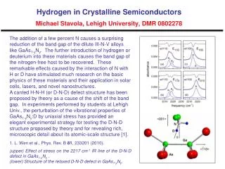
1 / 2
20 likes | 134 Views
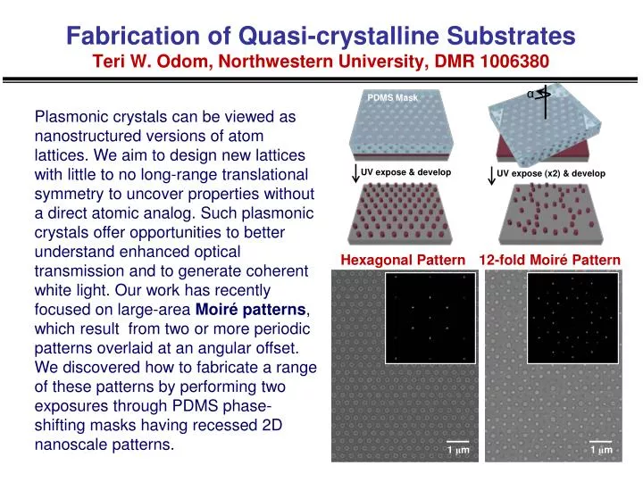
Fabrication of Quasi-crystalline Substrates Teri W. Odom, Northwestern University, DMR 1006380. α. PDMS Mask.

E N D
Fabrication of Quasi-crystalline SubstratesTeri W. Odom, Northwestern University, DMR 1006380 α PDMS Mask Plasmonic crystals can be viewed as nanostructured versions of atom lattices. We aim to design new lattices with little to no long-range translational symmetry to uncover properties without a direct atomic analog. Such plasmonic crystals offer opportunities to better understand enhanced optical transmission and to generate coherent white light. Our work has recently focused on large-area Moiré patterns, which result from two or more periodic patterns overlaid at an angular offset. We discovered how to fabricate a range of these patterns by performing two exposures through PDMS phase-shifting masks having recessed 2D nanoscale patterns. UV expose & develop UV expose (x2) & develop 1 µm Hexagonal Pattern 12-fold Moiré Pattern 1 µm 1 µm 1 µm 1 µm
Hands-on Nano Day at NorthwesternTeri W. Odom, Northwestern University, DMR 1006380 Photolithography Soft Lithography Annually, the Odom lab hosts hands-on demonstrations on nanotechnology for local high school students. This year, the students created their own photomasks and used them for photolithography. To learn soft nanolithography, they molded patterns onto transparent plastics and observed their diffraction patterns. Finally, the students analyzed the nano patterns that they fabricated using atomic force microscopy (AFM) and scanning electron microscopy (SEM). AFM Analysis SEM Imaging