Download
1 / 18
230 likes | 633 Views
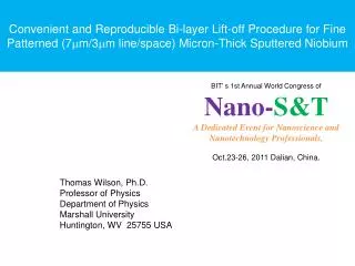
BIT' s 1st Annual World Congress of Nano- S&T A Dedicated Event for Nanoscience and Nanotechnology Professionals, Oct.23-26, 2011 Dalian, China. Convenient and Reproducible Bi-layer Lift-off Procedure for Fine Patterned (7 m m/3 m m line/space) Micron-Thick Sputtered Niobium .

E N D
BIT' s 1st Annual World Congress of Nano-S&T A Dedicated Event for Nanoscience and Nanotechnology Professionals, Oct.23-26, 2011 Dalian, China. Convenient and Reproducible Bi-layer Lift-off Procedure for Fine Patterned (7mm/3mm line/space) Micron-Thick Sputtered Niobium Thomas Wilson, Ph.D. Professor of Physics Department of Physics Marshall University Huntington, WV 25755 USA
Motivation: Thicker Niobium Grating-Coupler Required for Recently Developed Coherent THz LA Phonon Source “Phonon spectroscopy is a powerful technique for studying defects in materials and the properties of low-dimensional electrons and holes in semiconductors. A method of producing monochromatic phonon beams of usable intensity would revolutionize phonon spectroscopy …such a beam of phonons with nanometer wavelengths would be extremely useful for phonon spectroscopy of semiconductor nanostructures, e.g., quantum dots.” – A J Kent et al, Appl. Phys. Lett. 81, 3497 (2002).
Another potential application of coherent THz LA phonon source: Development of cryogenic acoustic microscope for sub-surface imaging with nanometer resolution … “3-D structure determination : “…sub-surface imaging and truly three-dimensional microscopy with nanometer-scale spatial resolution are not currently available; they are, however, extremely important for future development in nanotechnology. For example, most biological nanostructures are 3-D and currently imaged by X-ray crystallography, which is expensive and time-consuming. Even in nanoelectronics, which is progressing towards multilayer 3-D structures, 3-D imaging would be very useful. Possible approaches for subsurface imaging include ultrasonic echo imaging, non-linear (multiphoton) optical microscopy, and thermal spectroscopic imaging. It is unclear at present which, if any, technique would be suitable. This area clearly needs emphasis.” --- Interagency Working Group on Nano Science, Engineering, and Technology of the U.S. National Science and Technology Council, Vision for Nanotechnology Research and Development in the Next Decade (ISBN: 0792362209 )
Required components for coherent LA THz phonon generation by resonant absorption of grating-coupled THz laser radiation in Si doping-superlattices Nanosecond-pulsed multi-kW THz laser MBE silicon doping-superlattice with period equal to LA phonon wavelength at laser excitation frequency on Si:B substrate. Small-period grating-coupling required. (a) Detection: Fast, sensitive superconducting bolometer, shielded from scattered laser light. (b) Stress apparatus for phonon spectroscopy Low-temperature liquid helium immersion cryostat
Experiment: Generation of THz longitudinal acoustic phonons resonantly excited in Si-doping superlattices by pulsed laser radiation Uniaxial Stress Apparatus ( ~ 1-kBar) Front Face: Si Doping Superlattice (5 x 1012 cm-2) 246-GHz LA Phonon Si:B (5 x 1013 cm-3) Substrate ( Piezophonon Spectroscopy) Ultrashort-pulsed MM-Wave Laser Radiation ( 1.22-mm, 5-ns, ~ 50-kW ) 34.5-nm period Rear Face: Granular Aluminum Bolometer: Straight Link ( 100-nm x 10 micron x 20 micron) Front Face: Small-Period Niobium Grating Coupler (Line: 7 micron, Space: 3 micron) 5 x 7 x 0.5 mm Sample Immersed in LHe ~1.6K Grating-coupled evanescent longitudinal electric field in superlattice Transverse propagating electric field
Multi-kW ns-pulsed cavity-dumped molecular-gas terahertz laser
First Results: Bolometer Response(arbitrary units): Evidence of coherent LA phonon generation (8000 pulses averaged). Saturating leakage of larger cavity-dumped FIR pulse near 0 ns arrival of ballistic coherent LA phonons at expected TOF (65-ns) from cavity-dumped FIR laser low-level background FIR radiation leaking through grating-coupler striking absence of any larger delayed, incoherent TA phonon signal PHONONS2010
Bolometer Response(nW): Evidence of coherent LA phonon generation (8000 pulses averaged). Leakage of cavity-dumped FIR laser radiation through grating-coupler Arrival of ~ 2-nW ballistic coherent LA phonon signal at appropriate TOF and of same pulse width as generating cavity-dumped FIR laser Absence of any delayed larger, incoherent TA phonon signal –(expected if LA phonon signal was simply incoherent heat pulse) PHONONS2010
Related photolithography challenges (and use same developed process for both grating and bolometer fabrications) • Increase thickness of niobium grating > mm • Modify current image-reversed (maintain negative photomasks) AZ5214E lift-off process to include a PMGI lift-off resist (LOR) layer with a controlled undercut suitable for thicker niobium grating and aluminum bolometer fabrication • Continue use of meta-silicate (Na2SiO3 + Na3PO4) based developer (AZ Developer 1:1) to avoid etching of granular aluminum bolometer (NaOH-, KOH-, or TMAH-based developers attack aluminum at a rate of approx. 50-100 nm/min)
LOR-10B/Image-Reversed AZ5214E Bi-Layer Process Flow* • Procedure: (Use custom vacuum chuck for Laurell spinner with microfiltered syringes for dispense) • Piranha clean/HF dip for 12 mm x 16 mm silicon chips • Dehydration hot plate bake, 10 min at 200ºC • Spincoat 0.9 micron MicroChemLOR-10B (4000 RPM). (PMGI Platform) Soft bake 2 min at 150ºC. • Spincoat 1.3 micron MicroChemicalsAZ5214E (5000 RPM). Razor to remove edge bead. Soft bake 1 min at 100ºC. • Expose (Karl Suss MA6 mask aligner – soft contact mode) 60 mJ/cm2 • Reversal bake, 120ºC 1 min • Flood expose, 200 mJ/cm2 • Batch develop MicroChemicalsAZ Developer 1:1, 90 sec • Sputter niobium, 8.5 mT Ar, 30 sccm,100 W, 40 min • Lift-off in MicroChem Remover PG (NMP based solvent stripper), easily done (no sonication required) in 10-20 minutes. Rinse in IPA, then de-ion H20 (no acetone!) • * - Numerous details omitted of course
Schematic diagram of bi-layer lift-off resist process (with AZ Developer 1:1) 1. Double spin/Double bake/Expose bi-layer 3. Sputter Metal Layer 2. Image-Reversal Bake/Flood Expose/Develop 4. Lift-off of Photoresist
Optical micrograph of the 10 mm grating pattern with LOR-10B + AZ5214E bi-layer after development and before metal sputtering. Edges are smooth and straight. 10 micron period grating
Optical micrograph of the 10 mm grating pattern after lift-off of 1.2 mm thick sputtered niobium. Edges are not smooth. 10 micron period grating
SEM cross-section image of post-develop bi-layer profile Note: Negative sidewall of image-reversed AZ5214E and absence of LOR undercut AZ5214E LOR-10B spacer Substrate
SEM Cross-section image of after liftoff 1.2 mm thick sputtered niobium line 6.6 mm wide, 1.2 mm thick Nb grating line Undesirable metal fence/flags from resist sidewall coverage
SEM Image of Post-Liftoff of 1.2 mm thick, 10 mm period Nb grating 10 mm period niobium grating
Conclusions • A LOR/Image-Reversed AZ5214E Bi-Layer Photolithographic Lift-Off Process has been developed for thick (greater than 1 micron) sputtered metal. Process is reproducible and robust. Metal fence/flags not an issue for grating-coupler, nor for much thinner (100 nm) bolometer. New phonon measurements soon. • Improvements to process to remove flagging (as schematically depicted in above slide) expected with addition of a 2nd develop step. • Increase thickness with LOR-20B to 2 microns and increase bake temperature. • Decrease thickness of AZ5214E to 1 micron. • Increase exposure to 100 mJ/cm2 for vertical AZ 5214E sidewall • Add a 1 min 150ºC hot plate post-develop bake to reduce AZ dissolution rate, during a subsequent • 2ndAZ Developer (1-2 minutes?) develop (primarily only LOR dissolves here) step to generate a 500 nm undercut beneath AZ5214E
Acknowledgements • Marshall University COS and Department of Physics • NSF ECCS award 066260; US Army Research Office award DAAD19-01-0466, NASA EPSCoR award • Collaborators: Drs. Erich Kasper, Joerg Schulze, Michael Oehme (IHT, U-Stuttgart, FRG) Dr. Hans-Joachim Gossmann (Axcelis Technologies) silicon doping superlattices • West Virginia University ECE Nanofabrication Facility: Dr. Kolin Brown, Cleanroom Manager • Marshall University: Nathaniel Crow (undergraduate) and David Neff, SEM Imaging Technician


![[PDF] Free Download Space Opera By Catherynne M. Valente](https://cdn4.slideserve.com/8023580/slide1-dt.jpg)