Download
1 / 23
230 likes | 446 Views
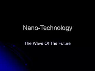
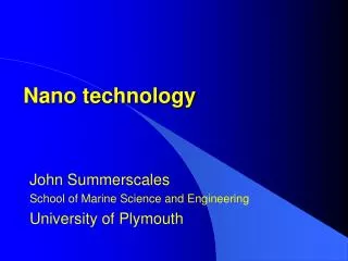
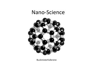
What is “Nano-scale Science and Technology”? Part II. Yonhua Tzeng, Professor Electrical and Computer Engineering Auburn University, Alabama USA. July 7, 2003. Thickness Effects. Gold Nanoshell.

E N D
What is “Nano-scale Science and Technology”? Part II Yonhua Tzeng, Professor Electrical and Computer Engineering Auburn University, Alabama USA July 7, 2003
Thickness Effects Gold Nanoshell Illustration of relative absorption of tissue components at various wavelengths, including the "tissue optical window". http://www.nanospectra.com/physics/physics.asp Calculated gold Nanoshell plasmon resonances for a 120nm core with the shell sizes shown.
Plasmon Resonance Plasmon resonances give to specific metallic nanoparticles a strong and well defined color. This effect was already used in the Middle Ages to fabricate stained-glass windows (left) and Greek vase (right). http://www.ifh.ee.ethz.ch/~martin/res50.en.html
Interfacial phenomena: Surface Plasmon Resonance Sensor http://www.cpac.washington.edu/~campbell/projects/spr.html http://icg.harvard.edu/~mcb169/Extras/SPR.htm
Quantum Mechanics: Quantum Corral http://www.wtec.org/loyola/nano/IWGN.Research.Directions/IWGN_rd.pdf
C60 SET Park et al., Nature 407, 57 (2000).
Quantum Tunneling Schematic presentation of Coulomb blockade and single electron tunnelling. (From Hitachi Cambridge Lab.)
Spintronics: Giant Magnetoresistance http://www.hgst.com/hdd/technolo/gmr/fig8.gif
Magnetic Tunneling Junction and MRAM MRAM developed by IBM and Infineon To write "1", IBM scientists simultaneously force one current to flow through the top electrode and another through the write word line; writing "0" requires the same process except that the current through the top electrode flows in the opposite direction. To read "1" and "0", the scientists force another lesser current to flow from the bottom electrode through the stack of magnetic layers and out the top electrode. The magnetic stack allows greater current flows to the top electrode for reading "1" than for reading "0". The red and green spheres represent electrons spinning in opposite directions in the magnetic layers. The very thin insulator allows electrons to quantum-mechanically tunnel through it. Information is stored in the top layer by forcing its electrons to spin in one direction or another. Information is retrieved by measuring the amount of current that travels through the tunnel insulator, which depends on the spin direction of the electrons in the top layer. http://domino.research.ibm.com/comm/bios.nsf/pages/mramvlsi.html http://domino.research.ibm.com/comm/bios.nsf/pages/mramvlsi.html/$FILE/mram.avi
Photonic Crystal - Tunable Please stretch yourself when we are doing research! Image from Prof. Z.Y. Cheng, Auburn University.
Biological systems Molecular motor http://www.wtec.org/loyola/nano/IWGN.Research.Directions/IWGN_rd.pdf
Polymer-Molecular Actuators Polymer Molecular Transistors ??? Image from Prof. Z.Y. Cheng, Auburn University.
Liquid Crystal Polymers Image from Prof. Z.Y. Cheng, Auburn University.
Biocompatible Quantum Dots New biocompatible quantum dots are set to revolutionize biological imaging. In (a) a frog embryo has been imaged using conventional organic-dye techniques, and the signal is seen to fade in time. (b) Specially prepared quantum dots that were injected into another frog embryo at the same time fluoresce brightly for much longer. http://physicsweb.org/article/world/16/3/3
Synthesis of composite polymer nanoparticles and hollow polymer nanocapsules for bioencapsulation and intracellular delivery (Feldheim group, UNC) A metal particle serves as a template for the formation of thin skins of polymer. Dissolution of the particle following polymer formation results in a hollow capsule. Small molecules or larger biomolecules (horseradish peroxidase, avidin, DNA) may be trapped in the hollow core simply by attaching the molecule of interest to the particle prior to polymer formation. Enymes maintain their activity inside the hollow polymer capsules and are even protected to a certain extent by denaturing agents such as organic solvents. A hollow polypyrrole capsule templated with a 200 nm diameter gold particle. http://www.ncsu.edu/chemistry/dlf/polymernano.html
Integration of “Nanostructures" at Micron-length and Macroscopic Scales Bottom-up Top-Down Bottom-up and top-down nanostructure synthesis and assembly approaches. http://www.wtec.org/loyola/nano/02_01.htm
Environmental • And Purification • Dispersions, Coatings, • and Other Large Surface • Area Structures Processing and Applications • Nanodevices, • Nanoelectronics, • and Nanosensors • Consolidated • Nanostructures • Biological, Medical, • and Health Energy and Chemicals http://www.wtec.org/loyola/nano/IWGN.Research.Directions/
Downloadable Proceedings http://www.wtec.org/loyola/pdf/nano.pdfand Technology
Downloadable Proceedings http://www.wtec.org/loyola/nano/IWGN.Research.Directions/IWGN_rd.pdf
The ITRI nanotechnology center led by ITRI Vice President J.C. Yang, will focus on 11 application areas of nanotechnology in the near term. These areas include • semiconductor chips, • information storage, • displays, • opto-communications, • electronics assembly, • platform technology, • testing and analysis equipment, • biotechnology, • energy and • traditional industries.
The center will budget NT$745 million (US$21.28 million) this year and NT$1.7 billion (US$48.57 million) next year for the research. • The center will open an 18,000-square-foot nanotechnology research lab at an old chip fabrication plant recently returned to ITRI by Taiwan Semiconductor Manufacturing Co. (TSMC). • Yang points out that commercialization of nanotechnology applications developed by the center will occur • first in • old economy industries: • painting, • dyeing, • printing, and • fiber and textile manufacturing. • Research on the traditional applications will take up around 20 percent of the center's resource and are expected to help these industries generate production value of around NT$90 billion (US$2.57 billion) in two to three years.