Download
1 / 11
110 likes | 225 Views
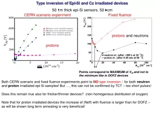
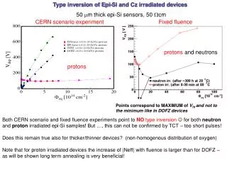
Type inversion of Epi-Si and Cz irradiated devices. 50 m m thick epi-Si sensors, 50 W cm. CERN scenario experiment. Fixed fluence. protons and neutrons. protons. Points correspond to MAXIMUM of V fd and not to the minimum like in DOFZ devices.

E N D
Type inversion of Epi-Si and Cz irradiated devices 50 mm thick epi-Si sensors, 50 Wcm CERN scenario experiment Fixed fluence protons andneutrons protons Points correspond to MAXIMUM of Vfd and not to the minimum like in DOFZ devices Both CERN scenario and fixed fluence experiments point to NO type inversion for both neutron and proton irradiated epi-Si samples! But …, this can not be confirmed by TCT – too short pulses! Does this remain true also for thicker/thinner devices? (non-homogenous distribution of oxygen) Note that for proton irradiated devices the increase of |Neff| with fluence is larger than for DOFZ – as will be shown long term annealing is very beneficial!
Annealing of epi-Si devices Devices are not inverted – reduction of Vfd at late stage annealing EPI-Si 50 mm device T=20oC DOFZ 50 mm device • Similar annealing behavior is obtained for standard DOFZ detectors irradiated below inversion point! • Vfd after ~1 year at 20oC is much lower than initial Vfd (~125V) for all fluences The long term annealing at RT reduces the Vfd of the detector!
Stable damage of Epi-Si sensors generation of acceptors during Long Term Annealing generation of donors – stable damage donor removal Nc<0: Generation of positive space charge: Good agreement for samples of different thicknesses Larger donor removal for neutron irradiated samples The positive stable damage can be compensated by annealing (STA and LTA)!
Short term and long term annealing • Short term annealing similar to DOFZ • Long term (reverse) annealing has two components: • 1st order component • gY1=2.6x10⁻²cm-1, tY1~ 1000min@ 60oC • 2nd order component • ~10 y at 20oC (depending on fluence) gY1>gc acceptors formed during annealing can compensate stable donors At high fluences detectors can have Neff~0 after annealing! The lifetime of epi-Si detectors at SLHC is not determined by Neffincrease with fluence!
5 4 0 1 1 4 4 - - 2 2 F F C C z z < < 1 1 0 0 0 0 > > = = 5 5 . . 5 5 8 8 x x 1 1 0 0 c c m m e e q q 1 1 4 4 - - 2 2 F F C C z z < < 1 1 0 0 0 0 > > = = 3 3 . . 7 7 9 9 x x 1 1 0 0 c c m m e e q q 4 5 0 1 1 4 4 - - 2 2 F F C C z z < < 1 1 0 0 0 0 > > = = 1 1 . . 7 7 0 0 x x 1 1 0 0 c c m m e e q q 1 1 4 4 - - 2 2 F F C C z z < < 1 1 0 0 0 0 > > = = 1 1 . . 0 0 2 2 x x 1 1 0 0 c c m m e e q q 3 6 0 ] V [ p 2 7 0 e d U i i n n v v e e r r t t i i e e r r t t 1 8 0 9 0 n n i i c c h h t t i i n n v v e e r r t t i i e e r r t t 0 0 . 1 1 1 0 1 0 0 1 0 0 0 1 0 0 0 0 t [ m i n ] Type inversion of irradiated Cz devices from F. Hönniger’s thesis, Hamburg inverted not inverted Sumitomo p+n Cz-Diodes: 1.2 kW cm, d= 280 mm, [Oi]=8.1e17 cm-3 • According to evolution of Vfd there is no change in SC sign in CERN scenario experiment • Complicated (no simple model) annealing varying for different samples from the same wafer! • Inversion during annealing investigated with TCT – there is a region for which it is difficult to determine the sign of SC. How do we define the sign of the space charge for non-homogenous Neff? (examples will be shown for proton irradiated Ocmetic (magnetic) Cz from Helsinki – 1.1 kWcm , 300 mm thick)
In case of low fluence the assumption of constant Neff is valid! HOLES ELECTRONS Cz – 1e14 Cz – 1e14 p+ p+ high ohmic resistance after irradiation Steep transition at U~VFD d d depleted depleted D D undepleted undepleted n+ n+ If the diode is inverted the picture is reversed!
Cz – Irradiated to 5e14 • Charge plots for electron and hole signals show that Neffis not constant! • Large hole signal (charge) already at low voltages – injection in electric field region
ELECTRONS HOLES Both electron and hole seems to be injected in high field region, but… what we measure/see is damped by trapping of the drifting charge - t 1 = I ( t ) N exp( ) v ( t ) , 0 , e h e h t D ´ eff e , h To derive the electric field profile/space charge sign you must take trapping into account!
HOLE SIGNALS t=4.2 ns trapping correction
How do we define sign of the space charge for non-homogeneous Neff? The larger of two regions with opposite space charge determines what we call “the sign of the space charge”
Comparison of corrected hole signals for Fz an Cz detector irradiated in parallel to 5e14p t=4.2 ns t=4.6 ns trapping correction Main junction in the front Main junction at the back Cz – not inverted Fz – “inverted”