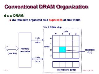
Accelerating DRAM Performance
Accelerating DRAM Performance. Bill Gervasi Chairman, JEDEC Memory Parametrics. RAM Evolution. 5400MB/s. DDR667. 4300MB/s. Mainstream Memories. DDR533. 3200MB/s. “DDR II”. DDR400. 2700MB/s. Simple, incremental steps. DDR333. 2100MB/s. “DDR I”. DDR266. Key to System Evolution.

Accelerating DRAM Performance
E N D
Presentation Transcript
Accelerating DRAM Performance Bill Gervasi Chairman, JEDEC Memory Parametrics
RAM Evolution 5400MB/s DDR667 4300MB/s MainstreamMemories DDR533 3200MB/s “DDR II” DDR400 2700MB/s Simple,incrementalsteps DDR333 2100MB/s “DDR I” DDR266
Key to System Evolution • Never over-design! • Implement just enough new features to achieve incremental improvements • Drive the hell out of the volumes to get the enhancements for free
New Specifications • DDR I • DDR333 chips • PC2700 MicroDIMM • PC2700 SO-DIMM • PC2700 Registered DIMM • PC2700 Unbuffered DIMM • DDR II • DDR400 chips • DDR533 chips • DDR667 chips • DIMM outline
DDR333 • 333 MHz data rate per pin • Approved for both TSOP and FBGA • First introduction of FBGA into SDRAM family • One package-dependent timing consideration! • Most improvements from tighter DLL design • Purpose of the DLL is accurate delivery of data and strobes during read cycles
DLL Effects CK • Clock jitter, pulse width distortion, DQS pull in or push out from pattern effects, p-channel to n-channel variation CK DDR266 = 750 psDDR333 = 600 ps tDQSCK* DQS
Data Capture Parameters • Data pin skew, simultaneous switching output effects, output driver variation • Note that data valid window width is package independent! DQS tDQSQ* tQHS* (simplified view) data DDR266 = 750 psDDR333 = 550 ps for TSOP = 600 ps for FBGA DDR266 = 750 psDDR333 = 450 ps for TSOP = 400 ps for FBGA
DDR II DDR400 SS800 DDR533 DDR667 Main System MemoryModules, etc Embedded ApplicationsPoint to Point
The DDR II Family • DDR II similarities to DDR I: • Compatible RAS/CAS command set & protocol • DDR II differences from DDR I: • DDR I = 2.5V, DDR II = 1.8V with calibration • Prefetch 4 • Differential data strobes • Improved command bus utilization: • Write latency as a function of read latency • Additive latency to help fill holes • New FBGA package & memory modules • Tighter package parasitics
DDR II Improves DDR I • Enables higher burst frequency • Makes better use of command slots • Lower voltage swing simplifies system concerns
DDR II Data Capture • Improvements from a combination of packaging, process, and voltage levels DQS tDQSQ* tQHS* (simplified view) data DDR400 = 450 psDDR533 = 400 ps DDR400 = 350 psDDR533 = 300 ps
Preparing for DDR II • Transitional controllers will need 2.5V or 1.8V selectable I/Os • Allocate pins for differential data strobe, tie one pin to VREF for DDR I mode • Use fixed burst length = 4 • Programmable write latency • WL = 1 for DDR I compliance • WL = Read Latency – 1 for DDR II compliance • Optional: additive latency
1.8V Signaling 2.5V VDDQ 1.8V 1.60V VDDQ VIHac 1.43V 1.15V VIHdc 1.25V VIHac VREF 1.03V VILdc VIHdc 1.07V 0.90V VREF VILac VILdc 0.77V 0.90V VILac 0.65V VSS VSS 0V SSTL_2 SSTL_18
I/O Calibration • Balance n- and p-channel driver strength • Protocol defined for initializing memory interface • Command tells the DRAM to hold signals in a state, controller overdrives and adjusts drive strength to match Data VTT Controller Data VREF DRAM
Differential Data Strobe • Just as DDR added differential clock to SDR • DDR II adds differential data strobe to DDR I • Transition at the crosspoint of DQS and DQS • Route these signals as a differential pair • Common mode noise rejection
Differential Data Strobe VREF DQS DQShigh time DQSlow time Normal balanced signal VREF DQS DQShigh time DQSlow time Mismatched Rise & Fall signal Error!
Differential Data Strobe DQS VREF DQS DQShigh time DQSlow time Normal balanced signal DQS VREF DQS DQShigh time DQSlow time Mismatched Rise & Fall signal Significantly reduced symmetry error
Moving to the Next Level • Today’s SDRAM architectures assume an inexpensive DRAM core timing • DDR I (DDR200, DDR266, and DDR333) prefetches 2 data bits: increase performance without increasing core timing costs • DDR II (DDR400, DDR533, DDR667) prefetches 4 bits internally, but keeps DDR double pumped I/O
Prefetch 2 Versus 4 CK READ data Prefetch 2 Core access time Prefetch 4 Costs $$$ Essentially free
So Why Not Prefetch 8 Now? • 64 bit bus widths are most practical tradeoff • Inexpensive 60 motherboards • 8 bytes per data cycle • Dropping to 32 bits or 16 bits raises system costs • Expensive 28 motherboards • Prefetch 8: lots of wasted data & bandwidth • Prefetch 8 means 64 bytes per access minimum on 64 bit bus
Additive Latency • Command slot availability is disrupted by CAS latency even on seamless read bursts • Sometimes with odd CAS latencies, sometimes with even • These collisions can be avoided by shifting READs and WRITEs in the command stream • Additive latency shifts R & W commands earlier – applies to both
Read Latency • In the past, data access from a READ command was simply CAS Latency • Combined with Additive Latency, ability to order commands better
Read & Additive Latencies CK ACT RD data CAS Latency CK ACT RD RL = AL + CL data Additive Latency CAS Latency
Write Latency • Complex controllers had collisions between command slots and data bus availability • These are eliminated in DDR II by setting Write Latency = Read Latency – 1 • Combined with Additive Latency, lots of flexibility in ordering commands
Write & Additive Latencies CK ACT WR data Additive Latency = 0 WL = RL – 1 CK ACT WR WL = AL + CL – 1 = RL – 1 data Additive Latency CL – 1
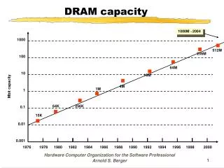
Summary • DRAM evolution continues • 266 333 400 533 667 MHz data rates • 2100 5400 MB/s throughput per module • Each step is a simple incremental improvement – without adding cost! • DDR II family adds a few new features • Lower voltage with I/O calibration • Differential data strobes • Command utilization improvements