Download
1 / 8
80 likes | 185 Views
Progress report on silicon and tungsten components, readout electronics status, and future timeline for experimental setup at Stanford Linear Accelerator Center. Key components and developments detailed. |

E N D
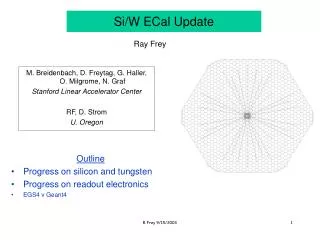
Si/W ECal Update Ray Frey M. Breidenbach, D. Freytag, G. Haller, O. Milgrome, N. Graf Stanford Linear Accelerator Center RF, D. Strom U. Oregon Outline • Progress on silicon and tungsten • Progress on readout electronics • EGS4 v Geant4 R Frey 9/15/2003
Component Status: W, Si, readout • W plates to make first full prototype arrive UO this week • 24 (20) plates, 25 mm x 6”x6”, 92.5% W, non-mag. • 12 (10) plates, 50 mm x 6”x6”, same alloy • Cu heat layer likely not needed – use the W to conduct • More study in progress • Silicon • Order for 10 prototype detectors sent to vendor today ! • Have readied test bench(es) to receive them (3 months) • Prep-ing with old (SSC vintage) detectors • Readout electronics • Each chip: 1000 x (analog, charge & time digit, calib., serial out) • Preliminary designs complete; need to fill in details; simulate • Conservative: increase channel footprint to 200m x 500m R Frey 9/15/2003
Ref Range Bit Cf High Gain Buffered High Range Output Shaper Ccal Buffered Low Range Output Low Gain VCal Logic Threshold Buffered Timing Signal Ramp Common Timing Ramp 200 ns 8.3 ms
Common Wilkinson Ramp Generator Wilkinson Scaler Scaler Bus 12 bits Threshold Timing Signal ADC Latch Threshold Latch (For Future zero suppression) Inputs from previous Page ADC Latch ADC Latch Output Buffer
Si detectors: revised metallization R Frey 9/15/2003
EGS Studies First: An old result 500 GeV electrons SD: 30 x 5/7 X0 SD vB: 20 x 5/7 X0 + 10 x 10/7 X0 R Frey 9/15/2003
Geant4 v EGS4 – First Look G4: test beam setup, N. Graf: 30x(W+G10+Si+G10+Cu+air), 5 GeV e- EGS4: same config. Total Energy deposited: ← EGS4 (MeV) G4: 4960 ± 40 MeV Energy dep. in silicon: ← EGS4 (MeV) G4: 66 ± 5 MeV R Frey 9/15/2003
Timeline (highly speculative) • 12/03: W and proto-Si in hand & undergoing tests • 12/03: readout chip design – complete 1st iteration • Winter 04: characterize detectors; prepare for B-field test • Readout few channels using external electronics • Spring 04: have first readout chips in hand • Summer 04: contemplate specialized tests in e- test beam • Electronics: heat, power pulsing, showers in chips • Detectors: resolution, noise, calibration • Summer 04: Next round of detectors and readout chips • Prepare for full-depth prototype • Fall 04: 1st bump-bonding trials • Winter 05: construct full-depth prototype for beam test(s) • In parallel, continue with simulations: • Technical: EGS4, G4 • Parameter optimizations based on PFlow R Frey 9/15/2003