Download
1 / 15
170 likes | 337 Views
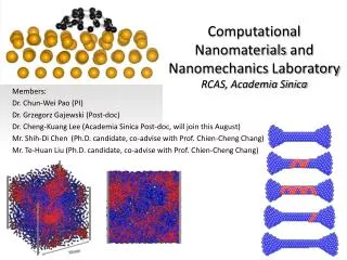
Computational Nanomaterials and Nanomechanics Laboratory RCAS, Academia Sinica. Members: Dr. Chun-Wei Pao (PI) Dr. Grzegorz Gajewski (Post-doc) Dr. Cheng- Kuang Lee (Academia Sinica Post-doc, will join this August)

E N D
Computational Nanomaterials and Nanomechanics LaboratoryRCAS, Academia Sinica Members: Dr. Chun-Wei Pao (PI) Dr. GrzegorzGajewski (Post-doc) Dr. Cheng-Kuang Lee (Academia Sinica Post-doc, will join this August) Mr. Shih-Di Chen (Ph.D. candidate, co-advise with Prof. Chien-Cheng Chang) Mr. Te-Huan Liu (Ph.D. candidate, co-advise with Prof. Chien-Cheng Chang)
Research Activities from July 2009 to Present • Atomistic simulations of tensile loading of Ag nanowires with strain rates close to experiments (manuscript in preparation) • Research conducted from July 2009 to September 2009 at Los Alamos National Lab., before joining RCAS • First atomistic simulation that can simulate nanoscale plasticity with atomistic resolution and experimental time scale • One contributed talk during TMS 2010 in Seattle, and one invited presentation in World Congress in Computational Mechanics in Sydney, Australia this coming July • Stress evolution during homoepitaxial growth of Cu with deposition rate close to experiments (manuscript in preparation) • Research conducted after joining RCAS, collaborating with Los Alamos and Univ. of Toledo • Demonstrate substantial compressive thin film growth stress even during homoepitaxial growth • Two invited seminars at National Taiwan Univ. and National Sun Yat-Sen Univ. this year
1.33 s 0.0 s 1.80 s 0.47 s <110> Rodrigueset al. PRB (2002) 2.17 s 1.23 s Ohnishi et al. Nature (1998) • Ag <110> nanowire • Nanowire thinned out uniformly Parallel-Replica Dynamics Simulation of Ag Nanowire Stretching • Au nanocontact formed by putting tip and sample together • # of rows of Au atoms reduced from 5 to 1 Performed massive parallel-replica dynamics simulations on Roadrunner supercomputer in Los Alamos National Lab. to simulate nanowire stretching processes with strain rates close to experiments
t=0.08ms dL=8Å t=0.06ms dL=6Å t=0.04ms dL=4Å t=0.02ms dL=2Å t=0.14ms dL=14Å Parallel-Replica Dynamics Simulation of Ag Nanowire Stretching t=0, dL=0 Replicate system into M replicas Dephasing trajectories Running independent trajectories t=0.12ms, dL=12Å
Stress Evolution during Homoepitaxial Growth Of Cu (001) during homoepitaxy growth, film growth Stress should be Friesen and Thompson, PRL 2004 However, it is reported that there exists correlations between surface roughness and thin film stress during homoepitaxial growth of Cu
Stress Evolution during Homoepitaxial Growth Of Cu (001) • Making use of the check board approach to extend the length scale of accelerated MD simulations • Will develop our own version this year Shim et al., PRB 2007 Deposition flux Run large-scale temperature accelerated dynamics simulations to simulate Cu homoepitaxial growth with deposition rate a million times slower than that in a typical direct MD simulation and monitor film stress evolution 60° Shim et al., PRL 2008; Paoet. al., in preparation
Stress Evolution during Homoepitaxial Growth Of Cu (001) • Asymmetrical film stress during 60° deposition simulation • Distribution of atomic virial stress shows relaxation of surface stress fxx at free surface in 60° deposition simulation
Stress Evolution during Homoepitaxial Growth Of Cu (001) • Since there is no absolute starting point for homoepitaxy, the film stress-thickness can be expressed as • Since homoepitaxy, no mismatch stress • Compute changes in surface stresses during growth and compare with simulations results and obtain excellent agreements
Ongoing and Future Research Projects • Surface chemical reactions during CVD growth of graphene on Cu substrate • Dr. GrzegorzGajewski • Graphene microstructures evolution • Mr. Te-Huan Liu • Nanoscale morphology evolution in the active layer materials of bulk heterojunction organic photovoltaic cells (NSC funded) • Dr. Cheng-Kuang Lee • Morphology evolution during annealing of C60 film • Mr. Shih-Di Chen • Development of accelerated MD codes for semi-empirical force fields and ab initio MD
Surface Chemical Reactions during CVD Growth of Graphene It is possible to fabricate large area of few-layer graphene by methane decomposition on Cu surface (Cu acts as catalysis) However, the surface chemical reaction pathways are not yet clear. Therefore, we are performing a series of ab initio calculations to study the surface chemical reactions Li et al., Science 2009 Li et al., Science 2009 Adsorption energy of a CH4 on Cu(111) is negligible (less than 0.005 eV), but, as will be shown later, once CH4 decomposes on Cu surface, the adsorption energies become much lower
Surface Chemical Reactions during CVD Growth of Graphene Adsorption energy and binding position on Cu(111) surface CH2 in fcc-top position d(Cu-C)= 2.000/2.079 Å d(C-H) = 1.104/1.117 Å CH in fcc position d(Cu-C)= 1.910 Å d(C-H) = 1.100 Å CH3 in hcp-top position d(Cu-C)= 2.239 Å d(C-H) = 1.109 Å
Surface Chemical Reactions during CVD Growth of Graphene Adsorption energy and binding position on Cu(111) surface add atom adsorbed on Cu(111) fcc position
Surface Chemical Reactions during CVD Growth of Graphene d(Cu-C)=2.137 Å d(Cu-H)=1.559 Å d(C-H) = 1.091/1.100 Å d(C.....H)=1.827 Å Eact=2.22 eV ΔH(CH4(g)→CH3(s)+H(s))= 0.78 eV ΔH(CH4(g)→CH3(s)+H(g))= 3.26 eV ΔH(CH4(g)→CH3(g)+H(g))= 4.72 eV Barrier of CH4 decomposition is tremendously lower on Cu surface Our preliminary results demonstrate: Adsorption energies decreases monotonically during CH4CH3CH2CH CH4 decomposition barrier is much lower on Cu surface than in the gas phase We will continue computing all the relevant transition state calculations and studying the reason why self-limiting growth happens
Grain Boundaries in Graphene Graphene domain boundaries can be used as metallic wire What about transport properties of other types of domain boundaries?? We plan to study the structures and transport properties of various domain boundaries in graphene, and study the migration mechanisms of these boundaries using accelerated MD in the future
Nanoscale Morphology Evolution in Bulk Heterojunction Organic Photovoltaic Cells Phase separation of PCBM:P3HT from preliminary coarsed-grain MD simulation result P3HT PCBM