Download
1 / 13
130 likes | 245 Views
This document provides an in-depth overview of the architecture of the ATLAS Pixel System, detailing its key components including sensors, frontend chips, and module control chips. It covers module design, connections, and pixel configurations in the pixel chips, including their dimensions and performance characteristics. Additionally, it discusses the evolution of the pixel chip series (FE-I1, FE-I2, FE-I3) and production metrics, as well as critical design issues and system tests conducted with mini-systems. The information is crucial for understanding the functionality and engineering behind the ATLAS Pixel System.

E N D
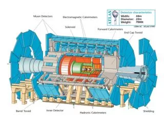
The ATLAS Pixel System Architecture • ATLAS Pixel Module: • 1 Sensor • 16 Frontend chips • 1 Module Control Chip (MCC) Module Stave / Disk Control Room
How does it look like? • Connections between FE-Chips, MCC, passive components and cable through a thin kapton PCB • Active area = 16.4 60.8 mm2 • 16 Chips with ~ 50000 pixels of 50 400 mm2 total • Larger pixels between chips
The ATLAS-Pixelsensors • n-in-n silicon • 250 mm thick • Normal pixels: • 50 × 400 mm2 • In interchip-regions: • Long pixels (600mm) • “Ganged” pixels
The ATLAS Pixelchips • Chip Size: 7.4 mm × 11 mm • 18 × 160 = 2880 Pixels • Pixel Size: 50 mm × 400 mm • Deep submicron, radiation hard (tested up to 60 Mrad) • 40 MHz operating frequency • Zero suppression in every pixel • Data is buffered until trigger arrives • Serial control and readout, LVDS IO • Analogue part: • ~ 40 mW power dissipation / pixel • ~ 200 e noise • Amplitude measured via pulse width (time over threshold)
The ATLAS Pixelcell • Constant current feedback • Leakage tolerance > 100 nA • Linear decay • Analogue information • Measure hit width • Individual Adjustment of • Threshold • Feedback • Adjust ranges • One pixel cell: in case of a charge above threshold address and Time over Threshold are read out Zero suppression in pixel
ATLAS Pixelchip-history / production • FE-I1: • Up to now 90 modules produced (90 % good modules) • Problems: • Problems with threshold dispersion / tuning • Inefficiencies (timewalk) in interchip-regions (longer / ganged pixels) • SEU-hardness not satisfactory (numbers?) • FE-I2: • Produced, modules built (numbers?), tested, irradiated • Problems of FE-I1 solved • Problems: • Race condition in digital part (global register) FE-I2.1, FE-I3 • FE-I3: • Production version, production expected to start end of this year • Module production: • Done by IZM (PbSn) and AMS (In) • ATLAS cut: Less than 150 bad pixels (0.3%) per module, less than 50 per chip
The Module Control Chip (MCC) • Interface between module and readout system • More or less equivalent to the pilot in our system • Receives commands from the readout system • Slow commands (config etc.) • Fast commands (during data taking, mainly for synchronisation issues) • Trigger command • Distributes commands and triggers to chips • Length of trigger can be configured from 25 – 400 ns • Minimum distance between two triggers 125 ns • Combines 16 individual events from the FE-chips
ATLAS Pixel Module - Connections • Command/Data Interface: 3/4 LVDS lines • DCI: Data & Command In • DTO/DTO2: Data Out, Data Out2 optional to increase bandwidth • CK: 40 MHz clock • Additional connections: • 1 High voltage • 2 Low voltages with sense-lines(?) • VDDD 2.0V for chips and MCC (0.8 – 1.5 A) • VDDA 1.7V (1.2 A) • CK Return for synchronisation • Backplane: Isolated
ATLAS Pixel Module - Dimensions • Thicknesses: Active area: 16.4 mm Module width: 22.4 mm Module length length of active area = 60.8 mm MCC: 180 mm Sensor: 250 mm FE-Chips: 180 mm (+ Kapton + passive components)
Possible Arrangements ~ 78 mm - overlap • 1-Plane setup • Dead areas: • Beam hole 2.2 × 0.6 cm • 2 bands of > 6 mm • Power per plane: ~16 W 61.2 mm • 2-Plane setup • Dead areas: • 1 band of 12 mm • Power per plane: ~ 8 W
Design issues • “Pigtail” • Flex cable connected to the kapton layer • Should (maybe) be designed by us, i.e. module should be delivered without • Form? (2D: routing of the lines, 3D: protection of the wire bonds) • Impedance issues, critical? • Connection: Wire bonds, soldering? • Ceramic / PCB • One piece or hybrid / ceramic? • Backplanes can / should be isolated • Behind/close to module no circuitry is needed, only heat conductivity • Lines impedance matched • Readout lines • Three LVDS lines (2 two module, 1 from module) • Maybe one return clock for synchronisation • Maximum length? • Power supply • Two power lines (per module ?) • Sense lines? (Note: digital current varies especially when module is noisy) • Readout • Protocol – difficult to implement in CFD readout-system?
ATLAS - Systemtests • First tests of mini-systems done: • 3 modules on a stave • 6 modules on a partial disk • Barrel setup (pigtail) looks close to something we could use …