Download
1 / 28
280 likes | 364 Views
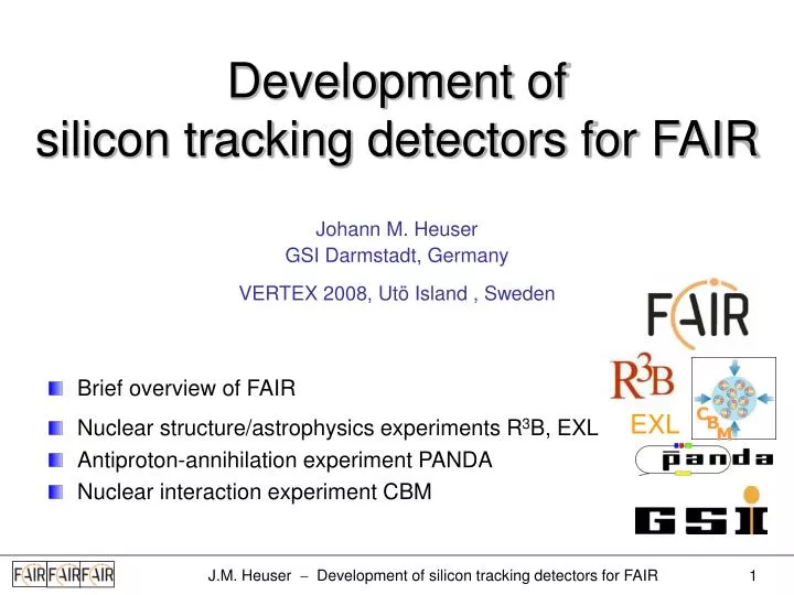
C. B. M. Development of silicon tracking detectors for FAIR. Johann M. Heuser GSI Darmstadt, Germany VERTEX 2008, Utö Island , Sweden. Brief overview of FAIR Nuclear structure/astrophysics experiments R 3 B, EXL Antiproton-annihilation experiment PANDA

E N D
C B M Development of silicon tracking detectors for FAIR Johann M. Heuser GSI Darmstadt, Germany VERTEX 2008, Utö Island, Sweden • Brief overview of FAIR • Nuclear structure/astrophysics experiments R3B, EXL • Antiproton-annihilation experiment PANDA • Nuclear interaction experiment CBM EXL J.M. Heuser Development of silicon tracking detectors for FAIR
Facility for Antiproton and Ion Research High-intensity primary and secondary beams Efficient parallel operation of up to 4 programs GSI German national laboratory for research with ions (in Darmstadt, south of Frankfurt) FAIR 2016 New international facility next to GSI J.M. Heuser Development of silicon tracking detectors for FAIR
Nuclear Structure & Nuclear Astrophysics Radiactive-ion beams from high-energy fragmentation QCD-Phase Diagram: Nuclear & QGP Matter Heavy-ion beams 2 to 45 GeV/u Hadron Structure, QCD-Vacuum & Medium Stored and cooled Anti-proton beams up to 15 GeV/c Fund. Symmetries & Ultra- High EM Fields Antiprotons and highly stripped ions Physics of Dense Bulk Plasmas Ion-beam bunch compr.+ high-energy petawatt-laser Materials Science, Radiation Biology Ion & anti-protonbeams Unprecedented research opportunities: FAIR http://www.gsi.de/fair Nov. 2001: FAIR Conceptual Design Report. Jul. 2002: FAIR recommended by german science council “Wissenschaftsrat“. Feb. 2003: FAIR approved by ministry of education and research "BMBF". Mar. 2006: Fed. Government: FAIR in budgetary plan up to 2014. Sept. 2006: FAIR Baseline Technical Report. Nov. 2007: FAIR Start-up event in 2008: Foundation of the FAIR Company 14 partner countries so far: First experiments: 2012 Completion in 3 phases: until 2016 Costs & Funding: Observers: ~1.2 billion € –65% Germany, 10% State of Hesse, 25% Int. Partners J.M. Heuser Development of silicon tracking detectors for FAIR
Start of the FAIR project on 7 November 2007 More than 1400 people attending the event. Austria, Germany, Spain, Finland, France, Poland, Romania, Russia, Sweden, Great Britain and german State of Hesse Officials from the FAIR partner states celebrating the launch of the start version. J.M. Heuser Development of silicon tracking detectors for FAIR
Facility for Antiproton and Ion Research SIS 100 SIS 300 p < 90 GeV SIS 18 ions up to U < 45 AGeV p-Linac CBM Unilac PANDA R3B GSI today New: Widespread application of high-performance silicon detector systems at FAIR! EXL FAIR 2016 J.M. Heuser Development of silicon tracking detectors for FAIR
EXLexperiment: experiment: "Reaction studies with Relativistic Radioactive Ion Beams" "EXotic Nuclei Studied in Light-Ion Induced Reactions" • Physics and programs • Structure of nuclear matter in its extreme states: Exotic nuclei • Physics for nuclear energy / nuclear data and modeling, astrophysics • Goals of the experiment • Complete reconstruction of the reaction kinematics with stable as well as radioactive beams • Beam energies: 150 MeV - 1.5 GeV per nucleon • Physics and programs • Nuclei far off stability • Exploring new regions in the chart of nuclides: paramount interest in the fields of nuclear structure and astrophysics • Goals of the experiment: • Complete reconstruction of light-ion induced direct reactions in inverse kinematics • Novel storage ring techniques and a universal detector system J.M. Heuser Development of silicon tracking detectors for FAIR
RIB Si Recoil Tracker High Resolution Measurement • 2-layer silicon tracker • ~ 0.2 m2 area • Target • Tracker • Calorimeter Neutrons Protons Heavy Fragments Large Acceptance Dipole • First layer: • double-sided Si micro-strip detectors • 2.5 cm from target, • thickness 100 μm, pitch 100 μm • energy resolution 50 keV (FWHM) • Second layer: • double-sided Si micro-strip detectors • 10 cm from target, • thickness 300 μm, pitch 100 μm • energy resolution 50 keV (FWHM) • The R3B experiment: • beam tracking and mom. measurement, Dp/p ~10-4 • exclusive measurement of the final state: • - identification and mom. analysis of fragments • (large acceptance mode: Dp/p~10-3, high-resolution mode: Dp/p~10-4) • - n, p, γ, light recoil particles • applicable to a wide class of reactions J.M. Heuser Development of silicon tracking detectors for FAIR
EXL Recoil detector Detection systems for: Target recoils and gammas (p,,n,…) Forward ejectiles (p,n,) Beam-like heavy ions • 2 nearly spherical silicon detector layers • ~3 m2 area. Si DSSD E, x, y 300 µm thick, spatial resolution better than 500 µm in x and y, ∆E = 30 keV (FWHM) Thin Si DSSD tracking <100 µm thick, spatial reso-lution better than 100 µm in x and y, ∆E = 30 keV (FWHM) Si(Li) E 9 mm thick, large area 100 x 100 mm2, ∆E = 50 keV (FWHM) CsI crystals E, High efficiency, high resolution, 20 cm thick RIB Electron cooler eA-Collider J.M. Heuser Development of silicon tracking detectors for FAIR
R3B: • 2-layer silicon tracker • ~ 0.2 m2 area • 60 microstrip detectors of about 5 cm by 7 cm size • Double-sided detectors with orthogonal strip pattern, read out from the same detector edge double-metal routing layer on one side. • Strip pitch: 100 µm or smaller. • Detectors thickness: 100 µm (inner layer), • 100-300 µm thickness (outer layers). • EXL: • 2 nearly spherical silicon layers • ~3 m2 area.. • Inner layer: 100 µm thick double-sided orthogonal microstrip detectors • Spatial resolution better than 100 µm in x and y • energy resolution of 30 keV. • 300 detectors with typical dimensions of 9 cm by 9 cm. • Outer layer: 300 µm thick double-sided orthogonal microstrip detectors • spatial resolution better than 500 µm in both coordinates. • energy resolution of 30 keV • 120 detectors of 9 cm by 9 cm size. • Detectors operated in vacuum. J.M. Heuser Development of silicon tracking detectors for FAIR
Anti-proton annihilation experiment PANDA • A next generation hadron physics detector • Cooled antiproton beams, energy 1.5 - 15 GeV, interacting with various internal targets. • Main physics topics: • hadron spectroscopy, search for exotic charmonia states • charm hadrons in the nuclear medium • spectroscopy of double-hypernuclei and nucleon structure. • PANDA detector system: • 4 acceptance, • vertex detection: MVD • particle id of Kaons, muons, e± • electromagnetic calorimetry • momentum resolution ~ δp/p = 1% • high interaction rates of up to 20 MHz J.M. Heuser Development of silicon tracking detectors for FAIR
Micro-Vertex Detector pellet or cluster jet target p beam 10 cm Experimental tasks: Identification of D mesons Measurement of long-lived baryons and mesons (open charm and strangeness) • Design features: • 5 space points forward of 90° • 4 barrel layers • 4 forward disks • Outer 2 barrels and disks: • double-sided strips, ~0.6m2 • Inner barrels and disks: • hybrid pixels • Smallest possible inner radius • Fast and untriggered readout J.M. Heuser Development of silicon tracking detectors for FAIR
Detector Prototyping Hybrid pixel detector layers: • Strip layers: • Outer layers: pixels strips: keep number of space points, but less material • double-sided sensors • thickness ~200 µm • orthogonal strips • pitch of 50 – 100 µm • typical barrel detector: 6 cm by 3.5 cm • lab-start: ITC detector, APV 25 chip • readout: untriggered FEE required • synergy with CBM on "XYTER" ASIC "TOPIX": .13 µ technology pixel size 100x100 µm2 high readout capability sufficient buffering to operate without trigger ToT to retain (some) energy information radhard within "typical" limits Sensor: EPI for minimum material: < 100 µm thickness J.M. Heuser Development of silicon tracking detectors for FAIR 12
PANDA MVD – Radiation load maps n-equiv. fluence/cm2, integrated over 1 year of PANDA operation pp at 10 GeV/c p-Pb at 4.05 GeV/c ~ 1/10 of radiation dose at LHC. calculation with DPM event generator J.M. Heuser Development of silicon tracking detectors for FAIR 13
Compressed Baryonic Matter Experiment • Fixed-target experiment at the SIS300 synchrotron • High-rate heavy-ion collisions, projectile energies up to 45 GeV/nucleon • QCD phase diagram in regions of large baryon densities and moderate temperatures • Topics: • Deconfinement phase transition and high-μB QGP. • Critical point. • Hadron properties in dense matter. • (rare) probes: e and µ pairs, vector mesons, strangeness and charmonium, open charm density dense nuclear matter: (6 – 12) 0 time J.M. Heuser Development of silicon tracking detectors for FAIR
Compressed Baryonic Matter Experiment Electron-Hadron setup Muon-setup J.M. Heuser Development of silicon tracking detectors for FAIR
Silicon Tracking System the mission ... ... tracking nuclear collisions • Au+Au interactions, 25 GeV/u, 10 MHz interaction rate • up to 1000 charged particles/event • Track densities 30 cm-2 UrQMD generator: Monte Carlo tracks ... + micro vertex detection: presentation by M. Deveaux ... and simulated hits in microstrip detector stations J.M. Heuser Development of silicon tracking detectors for FAIR
Exploration of a system concept STS: 8 low-mass micro-strip station 1 T dipole magnet J.M. Heuser Development of silicon tracking detectors for FAIR
r/o direction I II n side (back):"vertical" strips p side (front):"stereo" strips blue:double metal connect-ions of strips I to III III Tracking stations current layout: total area, 8 stations: 3.2 m2 total number of sectors: 756 total number of r/o channels: 1.5M total number of sensors: 1068188 sensors, 2 cm × 6 cm 166 sensors, 4 cm × 6 cm 714 sensors, 6 cm × 6 cm total number of FE chips: ~ 12k sector tracking station station with sectorization, max. 5% occupancy detector module double-sided microstrip detector J.M. Heuser Development of silicon tracking detectors for FAIR
Microstrip detector prototype CBM01, GSI-CIS 8/2007 Test sensors 4" wafer, 285 µm Si Double-sided, single-metal, 256256 strips, orthogonal, 50(80) µm pitch, size: 1515 (22 22)mm2 CBM01B1 CBM01B2 Main sensor Double-sided, double-metal, 1024 strips per side, 50 µm pitch, 15º stereo angle, full-area sensitive, contacts at top + bottom edge, size: 5656 mm2 CBM01 not rad hard J.M. Heuser Development of silicon tracking detectors for FAIR
Pixel vs. Strip detectors One central Au+Au event at 25 GeV/u, tracking station at z=30 cm track points : rec. points 1:1 track points : rec. points > 1:15 Y [cm] combinatorial hits true hits thin thick, cooling! current choice X [cm] compared with microstrip detectors hybrid pixel detectors J.M. Heuser Development of silicon tracking detectors for FAIR
Track reconstruction Front view (XY projection) Central collision: Au+Au @ 25 AGeV (UrQMD) Cellular automaton + Kalman filter algorithms 78 ms on Pentium 4 processor Future: farm of multi-core processors Reconstruction efficiency: 96% Top view (XZ projection) <1 % ghost tracks J.M. Heuser Development of silicon tracking detectors for FAIR
Low mass detector y[cm] x[cm] Station 5 ( at z = 60cm) X/X0 Momentum resolution • - silicon detector thickness: • currently 0.3% X0 (300mm) • station with cables and support • structure: 1% X0 1.3% for tracks pointing to the vertex J.M. Heuser Development of silicon tracking detectors for FAIR
Radiation Environment • Situation: • Interaction rate: 107/s Au+Au • Effective CBM run year: 2 months at full operation 5 × 10⁶ s FLUKA simulation: CBM cave neutron field STS dump beam 1-MeV nequiv fluence per 1 CBM run year: first STS station last STS station Typical operation: for about 6 years Fluenceup to ~1015 1-MeV nequiv. (Muon setup) J.M. Heuser Development of silicon tracking detectors for FAIR
Beginning STS system engineering • STS – MVD – beam pipein a thermal enclosure. • Extractable from the magnet for maintenance. • Including infrastructure (cables, optical links, cooling) 12k FEE chips 6 – 12 kW power FEE ASIC's operation at 1.8V current 3600 – 7200 A DAQ data rate ~30 GHz, ~200 GByte/s J.M. Heuser Development of silicon tracking detectors for FAIR
Summary • International accelerator facility FAIR under preparation: • Unprecedented and new research opportunities in various fields for large scientific communities • Silicon detector systems will be important • Challenging: • some because small research groups go into new detector dimensions • some because truly demanding devices are required: • very high channel densities, high radiation environment, very fast readout, very low mass, pretty big ( CBM) • Cooperations of the GSI/FAIR groups: e.g. on Sensors, FEE, labs • Input/advice from other experienced communities searched for: • One example: Planned are in-kind contributions from Finland to FAIR with rad-hard silicon strip detectors (incl. RD39-RD50 expertise) J.M. Heuser Development of silicon tracking detectors for FAIR
backup slides J.M. Heuser Development of silicon tracking detectors for FAIR
Name n-XYTER: Neutron - X, Y, Time and Energy ... Readout Front-end 128(32) channels, charge sensitive pre-amplifier, both polarities 30 pF detector capacitance, ENC 1000 e self-triggered, autonomous hit detection time stamping with 1 ns resolution (needed to correlate x-y views) Readout energy (peak height) and time information for each hit data driven, de-randomizing, sparsifying readout 32 MHz average hit rate 128 channel version (Si,GEM): ~ 250 kHz hit / channel 32 channel version (MSGC): ~ 1 MHz hit / channel n-XYTER readout ASICDETNI - GSI J.M. Heuser Development of silicon tracking detectors for FAIR
timewalkcomp. digitalFIFO tokencell peakdetect& hold analogFIFO timestampcounter tokenmanager outputdrivers n-XYTER Architecture self-trigger:latch amplitudelatch timestore in FIFOs PreAmp fast shaper comparator slow shaper 32 MHzreadoutrate 32 MHzreadoutrate peaking time fast: 20 ns slow: 140 ns 1 ns step J.M. Heuser Development of silicon tracking detectors for FAIR