Download
1 / 1
30 likes | 226 Views
MODIFICATION OF AZO THIN FILM PROPERTIES BY ANNEALING AND ION ETCHING. S. Flickyngerov á 1 , M. Netrvalov á 2 ,L. Pru šá kov á 2 , I. Novotn ý 1 , P. Š utta 2 , J.Kováč 1 jr., V. Tvaro ž ek 1.

E N D
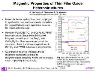
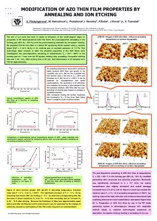
MODIFICATION OF AZO THIN FILM PROPERTIES BY ANNEALING AND ION ETCHING S. Flickyngerová1, M.Netrvalová2,L. Prušáková2, I. Novotný1, P.Šutta2 , J.Kováč1 jr., V. Tvarožek1 1Department of Microelectronics, Slovak University of Technology, Ilkovicova 3, 812 19 Bratislava, Slovakia, 2Department of Materials & Technology, New Technology Center, West Bohemian University, Univerzitni 8, 306 14 Plzen, Czech Republic The aim of our work has been to study an influence of two technological steps on properties of RF diode-sputtered AZO thinfilms: the post-deposition annealing in the forming gas (80% N2 / 20% H2) and the post-annealing treatment by ion-sputter etching.We prepared ZnO:Al thin films in a planar RF sputtering diode system using a ceramic target (ZnO+2 wt.% Al2O3) in Ar working gas at constant pressure of 1.3 Pa.Two technology steps (chosen to tailor the physical properties of the AZO films) were investigated:the post-deposition annealing at temperatures TA = 200 ÷ 400˚C in the forming gas for 1 hour and ion RF-sputter etching afterannealing. Ion-sputter etching rate was 7 nm/min. After etching time of 60 min. final thicknesses of all samples were 700 nm approximately. AFM 3D images of AZO thin films , influence annealing temperatureon surface topography RT 200°C An annealing temperatures above 200°C produced highly textured (002) films and growth of the crystallite size up to 400 nm The crystallite size had minimal value (100 nm) at TA = 200°C and increased up to 400 nm at TA = 400°C. It can be explained by recrystallization and phase transformations. The asymmetry of all diffraction lines indicates the forming of other phases at thin film-substrate interface. AZO films after the post-annealing ion-etching step showed no changes in crystalline structure. After ion-sputter etching the surface roughness has increased to Ra = 33 nm, three times higher value in comparison with no-etched sample. 300°C 400°C Optical transmittance spectra of AZO thin films as a function ofannealing temperature. RT 200°C a) b) Comparison of perpendicular optical transmission spectra of AZO / glass substrate and transmission spectra collectedbyintegrating sphere, both non post-depositon annealing (a) no etching (c) etched for 60min. 300°C 400°C AFM 3D images of AZO thin films,influence annealing temperature and ion etching on surface topography The post-deposition annealing of AZO thin films at temperatures TA = 200 ÷ 400 ˚C in the forming gas (80% N2 / 20% H2) modified particularly their structural and electrical properties. Resistivity was significantly decreased to 8 x 10⁻⁴cm, the optical transmittance also slightly decreased and optical bandgap increased from 3.15 eV to 3.36 eV. Figure of merit has reached the maximal value F = 8 % / Ω at annealing temperature of 400°C. Ion etching reduced the light reflection and enhanced disordered light scattering whereas the total transmittance maintained higher than 80 %. Preparation of AZO thin films by use of the RF diode sputtering system is advantageous becausethis adaptable method allows to combine technological sequences as deposition, ion-sputter etching, heating or annealing in one run. Influence of annealing temperature and ion etching on the figure of merit. Integral transmittance in the range of 400 – 1000 nm and calculated optical bandgap of AZO thin films after annealing at different temperatures. Figure of merit became greater with growth of annealing temperature, maximal value was F = 8 % / Ω at TA = 400°C . The significant increase of F (1 - 8 % / Ω) by annealing was lesser after ion etching (1 - 6 % / Ω) what was corresponding with the decrease of sheet resistance Rs from 75 – 10 Ω after annealing and an increase Rs to 80 – 18 Ω after etching. Because the thickness of films was approximately equal before and after etching the former phenomenon can, be explained by the change of resistivity caused by self-heating of thin film under long-term ion bombardment. Corresponding author: sona.flickyngerova@stuba.sk